ELECTRICAL TECHNOLOGY(ELECTRONICS) GRADE 12 MEMORANDUM - NSC PAST PAPERS AND MEMOS NOVEMBER 2021
Share via Whatsapp Join our WhatsApp Group Join our Telegram GroupINSTRUCTIONS TO THE MARKERS
- All questions with multiple answers imply that any relevant, acceptable answer should be considered.
- Calculations:
2.1 All calculations must show the formulae.
2.2 Substitution of values must be done correctly.
2.3 All answers MUST contain the correct unit to be considered.
2.4 Alternative methods must be considered, provided that the correct answer is obtained.
2.5 Where an incorrect answer could be carried over to the next step, the first answer will be deemed incorrect. However, should the incorrect answer be carried over correctly, the marker has to re- calculate the values, using the incorrect answer from the first calculation. If correctly used, the candidate should receive the full marks for subsequent calculations. - These marking guidelines are only a guide with model answers. Alternative interpretations must be considered and marked on merit. However, this principle should be applied consistently throughout the marking session at ALL marking centres.
MARKING GUIDELINES
QUESTION 1: MULTIPLE-CHOICE QUESTIONS
1.1 C (1)
1.2 B (1)
1.3 A (1)
1.4 D (1)
1.5 D (1)
1.6 A (1)
1.7 B (1)
1.8 B (1)
1.9 C (1)
1.10 B (A will also be accepted as correct) (1)
1.11 C (1)
1.12 B (1)
1.13 B (1)
1.14 B (1)
1.15 B (1)
[15]
QUESTION 2: OCCUPATIONAL HEALTH AND SAFETY
2.1
- To identify and communicate potential hazards
- To identify potential major incidents at the workplace to the employer.
OR - To review the effectiveness of health and safety measures.
- To investigate complaints by employees relating to health and safety at work. (2)
2.2
- Your right to earn a living wage.
- Your right to work for reasonable hours.
- Your right to belong to a trade union. (2)
2.3 An unsafe act is an action committed by a person which may lead to an accident or unsafe condition and/or loss.
An unsafe condition is a work related environmental condition which may lead to or contribute to an accident and/or loss. (2)
2.4
- High impact, low probability.
- High impact, high probability.
- Low impact, low probability.
- Low impact, high probability.
- Qualitative risk analysis.
- Quantitative risk analysis. (1)
2.5 'Danger' means anything that may cause injury to a person or damage to property. (2)
2.6
- Use an apron to protect your clothes from staining.
- Use protective glasses to protect your eyes.
- Use latex gloves to prevent skin irritation.
- Use a mask to reduce the risk of breathing fumes. (1)
[10]
QUESTION 3: RLC CIRCUITS
3.1 Capacitive reactance is the opposition of the capacitor to alternating current in an AC circuit. (2)
3.2 There is a 90° phase shift between VL and IL where IL lags VL by 90°. (1)
3.3 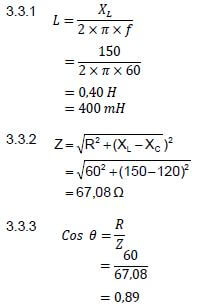
3.3.4
- R = Z
- Phase angle = 0°
- VL = VC
- XL = XC
- I is maximum (3)
3.4
3.4.1 800 Hz (1)
3.4.2 When the frequency increases from 200 Hz to 1600 Hz, the inductive reactance increases and the capacitive reactance decreases. (2)
3.4.3 ?? = ?? × X?
= 0,66 × 10−6 × 750
= 495 µ? (3)
3.4.4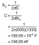
(3)
3.5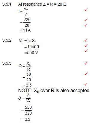
3.5.4 The phase angle would be zero because XL is equal to XC and thus VL = VC and out of phase with each other this would cancel each other, resulting in a power factor of 1.
R=Z
The circuit is at resonance (2)
[35]
QUESTION 4: SEMICONDUCTOR DEVICES
4.1 Enhancement Mode MOSFET. Depletion Mode MOSFET. (1)
4.2
4.2.1 P-channel enhancement mode metal oxide silicon field effect transistor (MOSFET). (1)
4.2.2 The MOSFET has a metal oxide layer which provides insulation between the gate electrode and the channel. In the JFET, the gate and the channel are physically connected together. (2)
4.3
4.3.1
- B2 - Saw tooth pulses
- Negative pulses (1)
4.3.2
- Saturation is when the operating point has fallen beyond the valley point when the emitter has been supplied with sufficient current.
OR - The saturation region is the permanent ON condition of the UJT after the valley point has been reached when the emitter was supplied with sufficient current. (2)
4.3.3
- The UJT is driven into the cut-off mode when the voltage across the capacitor falls to the UJT’s valley point, the emitter–base junction of the first transistor resets back to the high resistance , resulting in the UJT driven into the cut-off mode.
OR - When the emitter voltage falls to 0 V.
NOTE: the alternative response warrants 2 marks (3)
4.3.4 V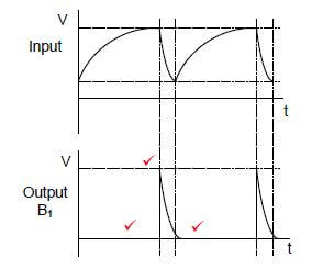
(3)
4.4
4.4.1 Darlington transistor amplifier. (1)
4.4.2 A supply voltage is connected between the collectors of the transistors and the emitter of transistor 2. When a voltage exceeding 1,4 V is connected to the base of the Darlington transistor, the transistors will be fully turned ON
NOTE: If the learner referred to the correct biasing method of the base- emitter and collector-emitter junctions, 2 marks will be awarded. (2)
4.4.3
- It can supply high current gain.
- Has improved input impedance and is less likely to load the preceding stages. (2)
4.4.4 A Darlington transistor is preferred over a single transistor as it is able to provide high current. It will energise and operate switching devices
that demand high current. (2)
4.5
4.5.1 Non-Inverting Operational Amplifier. (1)
4.5.2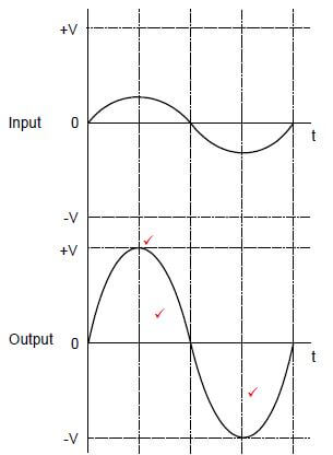
NOTE:
- 1 mark for amplification
- 2 marks for the correct waveform without distortion (3)
4.5.3 The differential amplifier only amplifies the difference in voltage between the two input signals. (1)
4.5.4
- The gain is reduced. (controllable)
- It stabilises the amplifier.
- Distortion of the output signal is reduced.
- Its bandwidth increases. (2)
4.6
4.6.1 It stores the information it last received until new information is received by using two stable states. (2)
4.6.2 + 5 V to (+15 V or +18 V). (2)
4.6.3 The three 5 kΩ resistors divide the supply voltage into three equal values that are used by the two comparators. (2)
4.6.4
- Astable Mode
- Monostable
- Bistable (2)
4.6.5 The pin monitors the voltage at which a 555 IC will trigger. When the threshold voltage (⅔ VCC) is exceeded, the IC will reset. (2)
4.7 The 741 Op-amp amplifies the difference between two inputs, therefore waveforms with equal amplitudes at the inputs would cancel each other leaving an output of zero (common mode rejection). (3)
4.8
4.8.1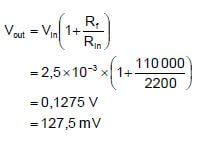
(3)
4.8.2 When the feedback resistance is equal to the input resistance the amplification factor will be 2 and the output voltage will be double the input voltage. (5 x 10⁻³ V) (2)
[45]
QUESTION 5: SWITCHING CIRCUITS
5.1
5.1.1 Resistor R1 is a pull up resistor keeping pin 2 high and the circuit in its stable state. (2)
5.1.2 0 V (1)
5.1.3 LED will be ON (1)
5.1.4 ±6 V
⅔ Vcc (1)
5.1.5 The duration of the train of on-off pulses during switch bounce are shorter than the charging cycle of the capacitor. Only when the capacitor has charged to point Y will the circuit change state. (2)
5.1.6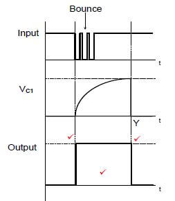
NOTE: 2 marks = 1 for each trigger point (the output must be a square wave)
1 mark = correct orientation (3)
5.2 5.2.1 Bistable multivibrator (1)
5.2.2 R2 provides feedback to the non-inverting input. (1)
5.2.3 Positive (1)
5.2.4
- When a positive pulse is applied to the input the voltage on both plates of the capacitor immediately rises to the magnitude of the input pulse.
- This is fed to the inverting input of the Op-amp.
- The Op-amp compares this voltage to the voltage at the non- inverting input and amplifies the difference.
- Its output is driven to negative saturation where it will remain. (4)
5.2.5
- When a negative voltage is applied the inverting input is still smaller than the voltage on the non-inverting input keeping the output positive.
- The output will only change state when a voltage greater (positive) than the voltage on the non-inverting input is applied to the inverting input. (2)
5.3
5.3.1 +1 V and -1 V (2)
5.3.2 The trigger voltage level is determined by the ratio of R1 to (R1+RF)
Trigger voltage (V+)= R1 ×Vout (1)
R1+RF
5.3.3 This circuit makes use of closed loop gain, because a portion of the output is fed back to the non-inverting input. (2)
5.3.4 Filters out unwanted noise from the input signal. Amplifies the input to a bigger output value. Changes the analogue input into a digital square wave. (2)
5.4
5.4.1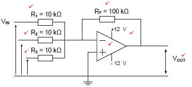
(7)
5.4.2 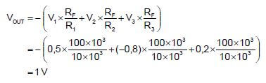
(3)
5.4.3 The polarity of the output voltage will become negative because the sum of the voltages at the input is positive. This positive value is then inverted and amplified by the inverting summing amplifier and changed into a negative output.
NOTE: If a learner correctly calculates the new output voltage and writes a concluding statement that the output changed to negative,
3 marks will be awarded. A calculation only, warrants 2 marks. (3)
5.5
5.5.1 R1, R2 (2)
5.5.2 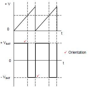
NOTE: 1 mark for orientation
1 mark for each correct trigger point (3)
5.6
5.6.1
- Improved input and output impedances.
- Boosts output gain. (Compensates for losses.)
- Added stability to the circuit. (2)
5.6.2 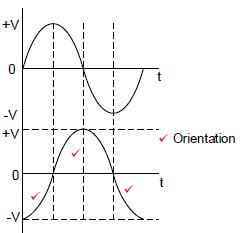
NOTE: 1 mark for orientation
1 mark for positive half cycle
2 marks for the correct negative half (4)
[50]
QUESTION 6: AMPLIFIERS
6.1
6.1.1 Class AB is a class of amplification where the output collector current will flow for more than 180o but less than 360o of the input cycle. (2)
6.1.2 Class C is a class of amplification where an output collector current will flow for less than 180o of the input cycle. (2)
6.2 Negative feedback means part of the output signal is fed back 180o out of phase with the input signal, thereby reducing the input signal. (2)
6.3
6.3.1
- It will set a limit to the maximum current flowing in the collector circuit and so protect the transistor from damage.
- It will set up a voltage drop across itself relative to amount of current flowing in the collector circuit. (1)
6.3.2 The coupling capacitors are selected around 10 µf values so that they can pass the audio range of frequencies from the input to the
output and block dc to protect the speaker and input devices. (2)
6.3.3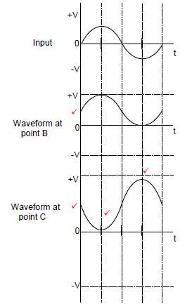
NOTE:
- 1 mark for DC offset and duplicate of the input at B
- 1 mark for the amplification at C
- 1 mark for DC offset at C
- 1 mark for correct waveform at C (4)
6.3.4 As the collector current (IC) through the transistor rises, the voltage across the collector-emitter voltage (VCE) resistor falls. (1)
6.3.5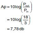
(3)
6.4
6.4.1 Hartley oscillator. (1)
6.4.2 Inductor (L1) and inductor (L2) or total inductance (LT) Capacitor (C3). (2)
6.4.3
- When switched ON, the transistor’s collector voltage rises and C1 starts charging.
- The change of the potential will appear across the inductor in an inverted form (1800 out phase), so driving the transistor’s base potential in the opposite direction, tending to switch off.
- This will enable the capacitor to discharge through the inductors and so push the tank circuit into oscillation.
- The flywheel effect of the tank circuit now begins to drive the transistor alternately 'ON' and 'OFF' which in turn continually re-charges the tank circuit in order to keep it oscillating at a constant frequency. (6)
6.4.4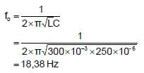
(3)
6.5
6.5.1 Two-stage transformer-coupled amplifier. (1)
6.5.2
- Transformer T1 serves as a coupling component between the two stages.
OR - Transformer T1 serves as an impedance matching component between the two stages. (1)
6.5.3 The primary coil’s resistance has a much lower value and therefore causes less dc power loss for the stage. (2)
6.5.4 Maximum power transfer would not take place and the output signal will be low. (2)
6.6
6.6.1 RC phase-shift oscillator. (1)
6.6.2
- There must be positive feedback that results in a combined 360o voltage phase shift around the circuit loop.
- The combined gain and loss through the amplifier and feedback network must be equal or slightly greater than unity.
OR - The energy fed back to the tuned circuit must be in phase with the first excitation voltage.
- The amplitude of the feedback voltage must be sufficient so that the energy dissipated by the resistance of the circuit is replaced.
- The value of C1, C2 and C3 must be equal.
- The value of R1, R2 and R3 must be equal. (2)
6.6.3 Positive feedback would help to overcome any attenuation in the feedback circuit and it will also drive the circuit into oscillation without a need for an input signal being applied. (3)
6.6.4
- Each set of RC network creates a phase-shift of 60° in the signal that passes through them that causes a total phase-shift of 180º
- Each set of the RC network acts as a voltage divider. (2)
6.6.5
- Attenuation is when the output voltage becomes smaller than the input voltage.
OR - (When a circuit causes a loss of signal power between its input and output it is said to have attenuated)
The reduction of the amplitude of a signal warrants 1 mark. (2)
[45]
TOTAL: 200