ELECTRICAL TECHNOLOGY(ELECTRONICS) GRADE 12 QUESTIONS - NSC PAST PAPERS AND MEMOS NOVEMBER 2021
Share via Whatsapp Join our WhatsApp Group Join our Telegram GroupINSTRUCTIONS AND INFORMATION
- This question paper consists of SIX questions.
- Answer ALL the questions.
- Answer the following questions on the attached ANSWER SHEETS:
QUESTION 4.3.4 and 4.5.2
QUESTION 5.1.6, 5.5.2 and 5.6.2
QUESTION 6.3.3 - Write your centre number and examination number on every ANSWER SHEET and hand them in with your ANSWER BOOK, whether you have used them or not.
- Sketches and diagrams must be large, neat and FULLY LABELLED.
- Show ALL calculations and round off answers correctly to TWO decimal places.
- Number the answers correctly according to the numbering system used in this question paper.
- You may use a non-programmable calculator.
- Calculations must include:
9.1 Formulae and manipulations where needed
9.2 Correct replacement of values
9.3 Correct answer and relevant units where applicable - A formula sheet is attached at the end of this question paper.
- Write neatly and legibly.
QUESTIONS
QUESTION 1: MULTIPLE-CHOICE QUESTIONS
Various options are provided as possible answers to the following questions. Choose the answer and write only the letter (A–D) next to the question numbers (1.1 to 1.15) in the ANSWER BOOK, e.g. 1.16 E.
1.1 Choose the correct example of an unsafe condition that is likely to cause damage to property or an injury:
- Running in the workshop
- Spilling liquid or oil without cleaning it up
- Faulty tools or equipment
- Overloading electrical outlets when connecting many appliances (1)
1.2 An RLC series circuit is predominantly inductive when …
- XC > XL
- XL > XC
- XL = XC
- VC > VL (1)
1.3 The phase angle of a predominantly capacitive RLC series circuit is …
- leading.
- lagging.
- in phase.
- zero. (1)
1.4 The … of a resonant circuit is the measure of how well it responds to a range of frequencies.
- conductance
- dissipation factor
- resonant frequency
- selectivity (1)
1.5 A bipolar junction transistor (BJT) is regarded as a/an … device.
- voltage-controlled
- drain-current (ID)
- insulation-gate type (IGBT)
- current-controlled (1)
1.6 The advantage of a field-effect transistor over a bipolar junction transistor is that it has a/an …
- extremely high input resistance.
- high input current.
- extremely low input resistance.
- low amplification factor. (1)
1.7 The N-channel JFET will operate correctly when the …
- gate-to-source pn-junction is forward biased.
- gate-to-source pn-junction is reverse biased.
- drain is connected to ground.
- gate is connected to the source. (1)
1.8 An astable multivibrator generates …
- one pulse cycle of high and low when a trigger pulse is applied.
- a continuous train of pulses without the need of a trigger pulse to be applied.
- one stable state without the trigger pulse being applied to its input.
- a sequence of triangular waveforms at the output. (1)
1.9 When applying a triangular waveform to the input of a differentiator, the output will be …
- a DC waveform.
- an inverted triangular waveform.
- a square waveform.
- the first harmonic of the triangular waveform. (1)
1.10 When the input voltage to a non-inverting Schmitt trigger is smaller than the reference voltage, the output is driven into ...
- positive saturation.
- negative saturation.
- both negative and positive saturation
- zero saturation. (1)
1.11 When a square wave is applied to the input of an op-amp integrator circuit, the output will be a …
- sine waveform.
- constant DC voltage.
- triangular waveform.
- square waveform. (1)
1.12 Choose the correct biasing method for a transistor amplifier:
The base-emitter junction is …
- reverse biased and the collector-base junction is forward biased.
- forward biased and the collector-base junction is reverse biased.
- forward biased and the collector-base junction is forward biased.
- reverse biased and the collector-base junction is reverse biased. (1)
1.13 The frequency range that occurs between the lower and upper frequencies in the frequency response curve of amplifiers is called the …
- critical frequency.
- midrange frequency.
- distortion frequency.
- decibel. (1)
1.14 In a class B amplifier, the collector current flows for …
- the whole of the input cycle.
- 180° of the input cycle.
- more than 180° but less than 360°.
- less than one half of the input cycle. (1)
1.15 An oscillator differs from an amplifier because the oscillator …
- has reduced gain.
- has a gain of 1 (unity).
- requires no DC supply.
- always has a changing output amplitude. (1)
[15]
QUESTION 2: OCCUPATIONAL HEALTH AND SAFETY
2.1 State TWO functions of a health and safety representative. (2)
2.2 Give TWO examples of human rights in the workplace. (2)
2.3 Differentiate between an unsafe act and an unsafe condition. (2)
2.4 Risk analysis can be divided into different categories. Name ONE category. (1)
2.5 Define danger with reference to the Occupational Health and Safety Act, 1993 (Act 85 of 1993). (2)
2.6 Name ONE personal protective item you would use when etching a printed circuit board (PCB). (1)
[10]
QUESTION 3: RLC CIRCUITS
3.1 Define capacitive reactance with reference to RLC circuits. (2)
3.2 State the phase relationship between the current and voltage in a pure inductive AC circuit. (1)
3.3 Refer to FIGURE 3.3 below and answer the questions that follow.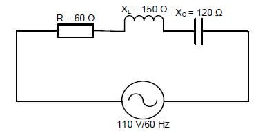
FIGURE 3.3: RLC SERIES CIRCUIT
Given:
R = 60 Ω
XC = 1 2 0 Ω
XL = 150 Ω
VT = 110 V
f = 60 Hz
3.3.1 Calculate the inductance of the inductor. (3)
3.3.2 Calculate the impedance of the circuit. (3)
3.3.3 Calculate the power factor. (3)
3.3.4 State THREE conditions that will occur if the power factor is at unity in a RLC series circuit. (3)
3.4 Refer to FIGURE 3.4 A and FIGURE 3.4 B below to answer the questions that follow.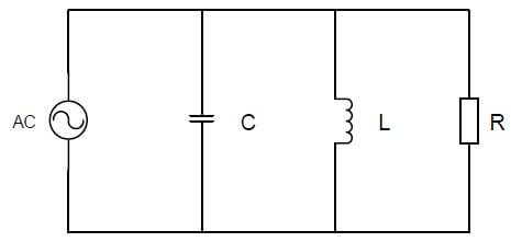
FIGURE 3.4 A: PARALLEL RESONANT CIRCUIT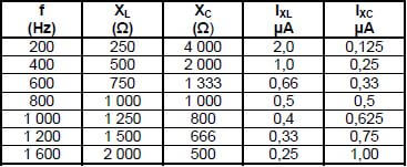
FIGURE 3.4 B: DATA OF THE RLC PARALLEL CIRCUIT
3.4.1 Determine the resonant frequency in FIGURE 3.4 B. (1)
3.4.2 Compare the values of the inductive reactance and capacitive reactance when the frequency increases from 200 Hz to 1 600 Hz. (2)
3.4.3 Calculate the voltage drop across the inductor when the frequency is 600 Hz. (3)
3.4.4 Calculate the value of the capacitor using the reactance value at 600 Hz. (3)
3.5 Refer to FIGURE 3.5 below and answer the questions that follow.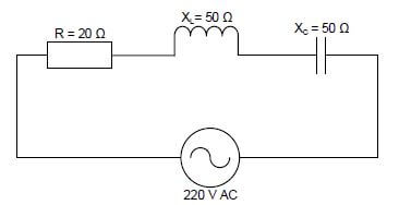
FIGURE 3.5: RLC SERIES CIRCUIT
3.5.1 Calculate the total current flow through the circuit. (3)
3.5.2 Calculate the voltage drop across the inductor. (3)
3.5.3 Calculate the Q-factor of the circuit. (3)
3.5.4 Explain why the phase angle of the circuit in FIGURE 3.5 would be zero. (2)
[35]
QUESTION 4: SEMICONDUCTOR DEVICES
4.1 Name ONE mode of operation of the metal-oxide-semiconductor field-effect transistor (MOSFET). (1)
4.2 Refer to FIGURE 4.2 below and answer the questions that follow.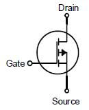
FIGURE 4.2: SEMICONDUCTOR SYMBOL
4.2.1 Identify the semiconductor symbol in FIGURE 4.2. (1)
4.2.2 Explain how the metal-oxide-semiconductor field-effect transistor (MOSFET) differs from the junction field-effect transistor (JFET) with reference to its construction. (2)
4.3 Refer to FIGURE 4.3 below and answer the questions that follow.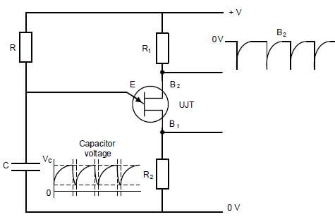
FIGURE 4.3: UJT PULSE GENERATOR
4.3.1 Identify pulses B2. (1)
4.3.2 Explain the term saturation region with reference to the operation of the UJT. (2)
4.3.3 Describe how the UJT is driven into the CUT-OFF mode. (3)
4.3.4 Draw the output voltage waveform across R2 on the ANSWER SHEET for QUESTION 4.3.4. (3)
4.4 Refer to FIGURE 4.4 below and answer the questions that follow.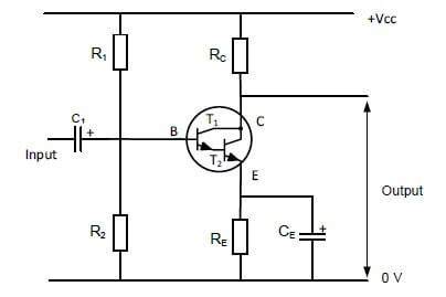
FIGURE 4.4: CIRCUIT DIAGRAM
4.4.1 Identify the circuit diagram in FIGURE 4.4. (1)
4.4.2 Describe how the transistors are biased and fully turned ON by referring to the required voltages. (2)
4.4.3 State TWO advantages of the circuit in FIGURE 4.4. (2)
4.4.4 Explain why the transistor in FIGURE 4.4 is preferred over a single transistor when used as a switch. (2)
4.5 FIGURE 4.5 below shows an operational amplifier. Answer the questions that follow.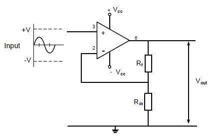
FIGURE 4.5: OPERATIONAL AMPLIFIER
4.5.1 Identify the type of operational amplifier in FIGURE 4.5. (1)
4.5.2 Draw the output voltage waveform on the ANSWER SHEET for QUESTION 4.5.2. (3)
4.5.3 Explain why operational amplifiers are known as differential voltage amplifiers. (1)
4.5.4 Give TWO reasons why negative feedback is important when the op amp is used as a linear amplifier. (2)
4.6 Refer to FIGURE 4.6 below and answer the questions that follow.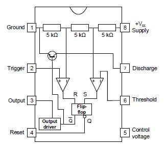
FIGURE 4.6: INTERNAL LAYOUT OF 555 TIMER IC
4.6.1 Explain the function of the RS flip-flop. (2)
4.6.2 State the typical operating voltage range of the 555 IC. (2)
4.6.3 Explain the function of the three 5 kΩ resistors inside the 555 IC. (2)
4.6.4 Name TWO modes of operation for the 555 IC. (2)
4.6.5 Explain the function of the threshold input on Pin 6 of a 555 IC. (2)
4.7 Refer to FIGURE 4.7 below and explain why the output is zero volts.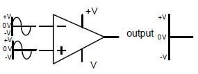
FIGURE 4.7: 741 OP AMP (3)
4.8 Refer to FIGURE 4.8 below and answer the questions that follow.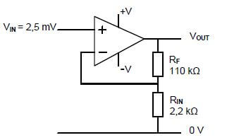
FIGURE 4.8: OP AMP
Given:
VIN = 2,5 mV
RIN = 2,2 kΩ
RF = 110 kΩ
4.8.1 Calculate the output voltage. (3)
4.8.2 Explain the effect on the output when the value of the feedback resistor is equal to that of the input resistor. (2)
[45]
QUESTION 5: SWITCHING CIRCUITS
5.1 Refer to FIGURE 5.1 below and answer the questions that follow.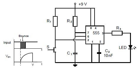
FIGURE 5.1: MONOSTABLE MULTIVIBRATOR
5.1.1 State the function of resistor R1. (2)
5.1.2 Write down the voltage across Pin 2 when switch S is pressed. (1)
5.1.3 State whether the LED will be ON or OFF when switch S is pressed. (1)
5.1.4 Determine the typical threshold voltage of the circuit. (1)
5.1.5 Explain why the switch bounce does not affect the output of the circuit. (2)
5.1.6 Draw the output on the ANSWER SHEET for QUESTION 5.1.6. (3)
5.2 Refer to FIGURE 5.2 below and answer the questions that follow.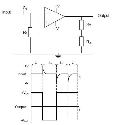
FIGURE 5.2: MULTIVIBRATOR
5.2.1 Identify the multivibrator circuit in FIGURE 5.2. (1)
5.2.2 State the function of resistor R2. (1)
5.2.3 Determine the polarity of the voltage on the non-inverting input during t1. (1)
5.2.4 Explain the operation of the circuit when a positive pulse is applied to the input. (4)
5.2.5 Explain why the output remains positive even after the pulse at t4 is applied. (2)
5.3 Refer to FIGURE 5.3 below and answer the questions that follow.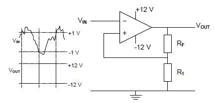
FIGURE 5.3: INVERTING SCHMITT TRIGGER
5.3.1 Identify the value of the trigger voltage levels. (2)
5.3.2 State how the trigger voltage level is determined. (1)
5.3.3 Explain whether the circuit uses open-loop or closed-loop gain. (2)
5.3.4 State TWO functions of the circuit. (2)
5.4 A summing amplifier consists of the following components:
NOTE: R1, R2 and R3 are input resistors. RF is a feedback resistor.
5.4.1 Draw the circuit diagram. (7)
5.4.2 Calculate output voltage if the following DC voltages are applied to the input resistors:
V1 = +0,5 V
V2 = -0,8 V
V3 = +0,2 V
(3)
5.4.3 Explain how the polarity of the output will be affected if the input voltage V3 is increased to V3 = +0,4 V. (3)
5.5 Refer to FIGURE 5.5 below and answer the questions that follow.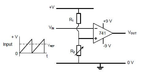
FIGURE 5.5: COMPARATOR
5.5.1 Name the components that determine the reference voltage. (2)
5.5.2 Draw the output voltage on the ANSWER SHEET for QUESTION 5.5.2. (3)
5.6 Refer to FIGURE 5.6 below and answer the questions that follow.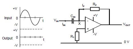
FIGURE 5.6: OP-AMP DIFFERENTIATOR
5.6.1 State TWO advantages of changing a passive differentiator to an active differentiator. (2)
5.6.2 Draw the output voltage on the ANSWER SHEET for QUESTION 5.6.2. (4)
[50]
QUESTION 6: AMPLIFIERS
6.1 Explain the following classes of amplifiers:
6.1.1 AB (2)
6.1.2 C (2)
6.2 Define the term negative feedback with reference to amplifier circuits. (2)
6.3 Refer to FIGURE 6.3 below and answer the questions that follow.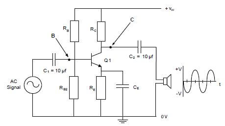
FIGURE 6.3: RC-COUPLED AMPLIFIER
6.3.1 State ONE function of the collector resistor (Rc). (1)
6.3.2 Explain why the coupling capacitors are purposely selected around the 10 μf values in FIGURE 6.3. (2)
6.3.3 Draw the waveforms that would be produced at point B and point C on the ANSWER SHEET for QUESTION 6.3.3. (4)
6.3.4 Describe the relationship between the collector current and the collector-emitter voltage when the input signal becomes positive. (1)
6.3.5 Calculate the power gain in decibels for FIGURE 6.3 if a 3-watt signal enters the amplifier and produces 18 watts at the speaker. (3)
6.4 Refer to FIGURE 6.4 below and the answer the questions that follow.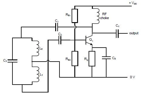
FIGURE 6.4: OSCILLATOR CIRCUIT DIAGRAM
Given:
LT = 300 mH
C1 = 250 μF
6.4.1 Identify the circuit diagram in FIGURE 6.4. (1)
6.4.2 Identify the components that determine the oscillation frequency in the circuit. (2)
6.4.3 Explain the operation of the circuit diagram. (6)
6.4.4 Calculate the oscillation frequency of the circuit in FIGURE 6.4 if the tank circuit has a total inductance of 300 mH and capacitor C3 has a capacitance of 250 μF. (3)
6.5 Refer to FIGURE 6.5 below and answer the questions that follow.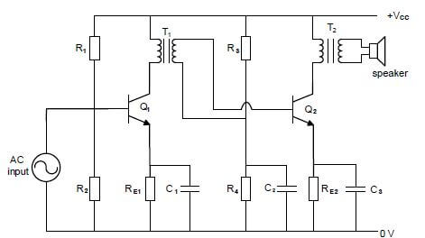
FIGURE 6.5: CIRCUIT DIAGRAM
6.5.1 Identify the circuit diagram in FIGURE 6.5. (1)
6.5.2 State the function of transformer T1. (1)
6.5.3 Describe why transformer T1 in FIGURE 6.5 is more efficient than using an RC stage for this amplifier. (2)
6.5.4 State the effect when the output impedance of transformer T2 is
NOT matched with the impedance of the speaker. (2)
6.6 Refer to FIGURE 6.6 below and answer the questions that follow.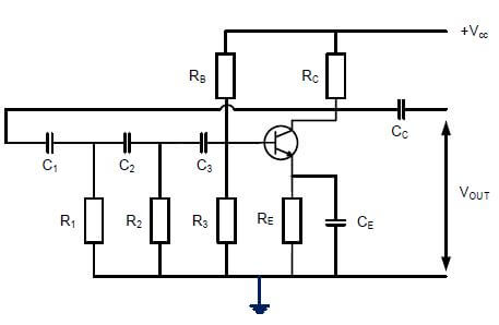
FIGURE 6.6: OSCILLATOR CIRCUIT
6.6.1 Identify the type of oscillator in FIGURE 6.6. (1)
6.6.2 State TWO requirements for oscillation to take place. (2)
6.6.3 Explain why the oscillator circuit in FIGURE 6.6 requires positive feedback to function. (3)
6.6.4 State TWO functions of the RC-network. (2)
6.6.5 Explain the term attenuation. (2)
[45]
TOTAL: 200
FORMULA SHEET
RLC CIRCUITS SEMICONDUCTOR DEVICES
ANSWER SHEETS
QUESTION 4: SEMICONDUCTOR DEVICES
4.3.4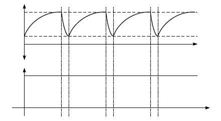
FIGURE 4.3.4 (3)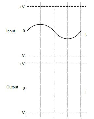
FIGURE 4.5.2 (2)
QUESTION 5: SWITCHING CIRCUITS
5.1.6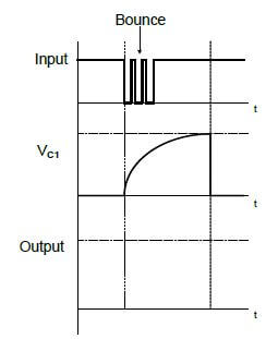
FIGURE 5.1.6 (3)
5.5.2 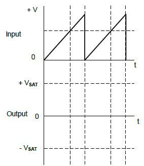
FIGURE 5.5.2 (3)
5.6.2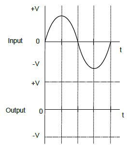
FIGURE 5.6.2 (4)
QUESTION 6: AMPLIFIERS
6.3.3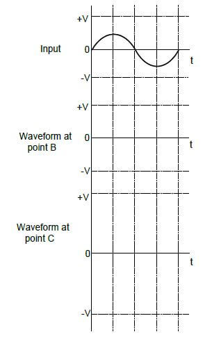
FIGURE 6.3.3 (4)