ELECTRICAL TECHNOLOGY(DIGITAL) GRADE 12 MEMORANDUM - NSC PAST PAPERS AND MEMOS NOVEMBER 2021
Share via Whatsapp Join our WhatsApp Group Join our Telegram GroupINSTRUCTIONS TO THE MARKERS
- All questions with multiple answers imply that any relevant, acceptable answer should be considered.
- Calculations:
2.1 All calculations must show the formulae.
2.2 Substitution of values must be done correctly.
2.3 All answers MUST contain the correct unit to be considered.
2.4 Alternative methods must be considered, provided that the correct answer is obtained.
2.5 Where an incorrect answer could be carried over to the next step, the first answer will be deemed incorrect. However, should the incorrect answer be carried over correctly, the marker has to re- calculate the values, using the incorrect answer from the first calculation. If correctly used, the candidate should receive the full marks for subsequent calculations. - These marking guidelines are only a guide with model answers. Alternative interpretations must be considered and marked on merit. However, this principle should be applied consistently throughout the marking session at ALL marking centres.
MARKING SCHEME
QUESTION 1: MULTIPLE-CHOICE QUESTIONS
1.1 C (1)
1.2 B (1)
1.3 C (1)
1.4 B (A will also be accepted as correct) (1)
1.5 C (1)
1.6 C (1)
1.7 D (1)
1.8 A (1)
1.9 C (1)
1.10 A (1)
1.11 D (1)
1.12 A (1)
1.13 C (1)
1.14 B (1)
1.15 D (1)
[15]
QUESTION 2: OCCUPATIONAL HEALTH AND SAFETY
2.1
- To identify and communicate potential hazards
- To identify potential major incidents at the workplace to the employer.
OR - To review the effectiveness of health and safety measures.
- To investigate complaints by employees relating to health and safety at work. (2)
2.2
- Your right to earn a living wage.
- Your right to work for reasonable hours.
- Your right to belong to a trade union. (2)
2.3 An unsafe act is an action committed by a person which may lead to an accident or unsafe condition and/or loss.
An unsafe condition is a work related environmental condition which may lead to or contribute to an accident and/or loss. (2)
2.4
- High impact, low probability.
- High impact, high probability.
- Low impact, low probability.
- Low impact, high probability.
- Qualitative risk analysis.
- Quantitative risk analysis. (1)
2.5 'Danger' means anything that may cause injury to a person or damage to property. (2)
2.6
- Use an apron to protect your clothes from staining.
- Use protective glasses to protect your eyes.
- Use latex gloves to prevent skin irritation.
- Use a mask to reduce the risk of breathing fumes. (1)
[10]
QUESTION 3: SWITCHING CIRCUITS
3.1
3.1.1 Resistor R1 is a pull up resistor keeping pin 2 high and the circuit in its stable state. (2)
3.1.2 0 V (1)
3.1.3 LED will be ON (1)
3.1.4 ±6 V
⅔Vcc (1)
3.1.5 The duration of the train of on-off pulses during switch bounce are shorter than the charging cycle of the capacitor. Only when the capacitor has charged to point Y will the circuit change state. (2)
3.1.6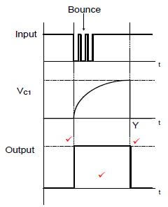
NOTE: 2 marks = 1 for each trigger point (the output must be a square wave)
1 mark = correct orientation (3)
3.2
3.2.1 Bistable multivibrator (1)
3.2.2 R2 provides feedback to the non-inverting input. (1)
3.2.3 Positive (1)
3.2.4
- When a positive pulse is applied to the input the voltage on both plates of the capacitor immediately rises to the magnitude of the input pulse.
- This is fed to the inverting input of the Op-amp.
- The Op-amp compares this voltage to the voltage at the non- inverting input and amplifies the difference.
- Its output is driven to negative saturation where it will remain. (4)
3.2.5
- When a negative voltage is applied the inverting input is still smaller than the voltage on the non-inverting input keeping the output positive.
- The output will only change state when a voltage greater (positive) than the voltage on the non-inverting input is applied to the inverting input. (2)
3.3
3.3.1 +1 V and -1 V (2)
3.3.2 The trigger voltage level is determined by the ratio of R1 to (R1+RF)
Trigger voltage (V+)= R1 × Vout (1)
R1+RF
3.3.3 This circuit makes use of closed loop gain, because a portion of the output is fed back to the non-inverting input. (2)
3.3.4 Filters out unwanted noise from the input signal. Amplifies the input to a bigger output value. Changes the analogue input into a digital square wave. (2)
3.4
3.4.1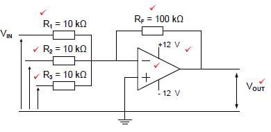
(7)
3.4.2 VOUT = -[V1 x RF/R1 + V2 x RF/R2 + V3 x RF/R3]
= - (0,5 x 100 x 103 + (-0,8) x 100 x 103 + 0,2 x 100 x 103)
10 x 103 10 x 103 10 x 103
= 1V (3)
3.4.3 The polarity of the output voltage will become negative because the sum of the voltages at the input is positive. This positive value is then inverted and amplified by the inverting summing amplifier and changed into a negative output.
NOTE: If a learner correctly calculates the new output voltage and writes a concluding statement that the output changed to negative, 3 marks will be awarded. A calculation only, warrants 2 marks. (3)
3.5
3.5.1 R1, R2 (2)
3.5.2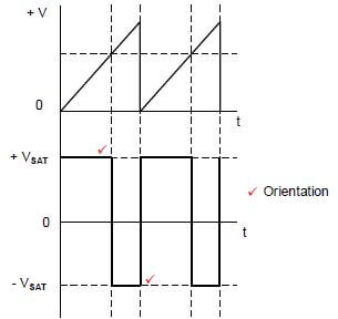
NOTE: 1 mark for orientation
1 mark for each correct trigger point (3)
3.6
3.6.1
- Improved input and output impedances.
- Boosts output gain. (Compensates for losses.)
- Added stability to the circuit. (2)
3.6.2 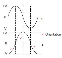
NOTE: 1 mark for orientation
1 mark for positive half cycle
2 marks for the correct negative half (4)
[50]
QUESTION 4: SEMICONDUCTOR DEVICES
4.1
4.1.1 Non-Inverting Operational Amplifier. (1)
4.1.2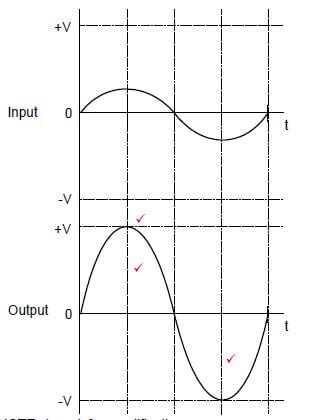
NOTE: 1 mark for amplification
2 marks for the correct waveform without distortion (3)
4.1.3 It is because it amplifies the difference between the two inputs signals. (1)
4.1.4
- The gain is reduced (controllable)
- It stabilises the amplifier
- Distortion of the output signal is reduced.
- Its bandwidth increases (2)
4.2
4.2.1 It stores the information it last received until new information is received by using two stable states. (2)
4.2.2 + 5 V to (+15 V or +18 V). (2)
4.2.3 The three 5 kΩ resistors divide the supply voltage into three equal values that are used by the two comparators. (2)
4.2.4
- Astable Mode
- Monostable
- Bistable (2)
4.2.5 The pin monitors the voltage at which a 555 IC will trigger. When the threshold voltage (⅔ VCC) is exceeded, the IC will reset. (2)
4.3 The 741 Op-amp amplifies the difference between two inputs, therefore waveforms with equal amplitudes at the inputs would cancel each other leaving an output of zero (common mode rejection). (3) [20]
QUESTION 5: DIGITAL AND SEQUENTIAL DEVICES
5.1 The cathodes of all eight LED's are internally connected to a 0 V or common ground. (2)
5.2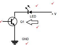
(5)
5.3
5.3.1 An encoder accepts the input data in a decimal format and converts it to binary format (3)
5.3.2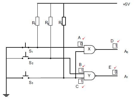
(5)
5.4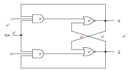
NOTE: 1 mark for both inputs
1 mark for both outputs
1 mark for each gate (x 4)
2 marks for the Latch
1 mark for the Clock
OR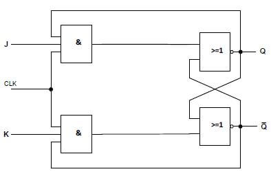
(9)
5.5.1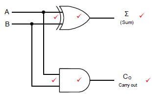
NOTE: 1 mark for inputs to the exclusive-OR gate
1 mark for inputs to the AND gate
1 mark for Sum (∑) 1 mark for Co
1 mark for each gate (x 2)
OR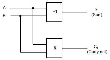
(6)
5.5.2
| INPUTS | OUTPUTS | ||
| A | B | ∑ | C0 |
| 0 | 0 | 0 | 0 |
| 0 | 1 | 1 | 0 |
| 1 | 0 | 1 | 0 |
| 1 | 1 | 0 | 1 |
(3)
5.6
- Frequency divider
- Decade Counter
- Binary Coded decimal (BCD) counter (2)
5.7
- A full sequence counter is a counter that runs to its maximum count.
- A truncated counter is a counter that is modified to stop its count before reaching its maximum count. (2)
5.8 Positive edge triggering is when the circuit reacts to the positive (or leading) edge of the pulse which rises from 0 to 1. (2)
5.9
- On beginning a count, FF0 and FF2 outputs feed the input of the NAND gate with a low '0'
- this means that the gate's output will be high '1' and it is this high '1' that enables the counter to begin operating as a normal 'up' counter.
- It continues with the up-count until reaching the binary output number 1012 (decimal 5).
- At this point both Q0 and Q2 outputs are high '1' which feed the input of the NAND gate, causing its output to fall to low '0'.
- This low '0' immediately disables the first flip-flop FF0
- preventing it from responding to any further input clock pulses.
- This effectively stops the counter, placing it on hold in the 1012 (510) state until a further reset signal is introduced.
NOTE: The circuit as taken from the textbook will not operate correctly and the answer given in this marking guideline will be accepted as it is in the official textbook.
Learners who indicated that the counter would jump from five (1012) to seven (1112) will be credited. (8)
5.10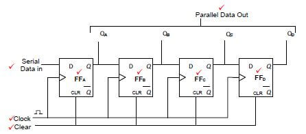
NOTE: 1 mark for Serial data input
1 mark for Parallel data output
1 mark for each labelled flip-flop (x 4)
1 mark for the Clear
1 mark for the Clock (8)
[55]
QUESTION 6: MICROCONTROLLERS
6.1
- A microcontroller is a single chip (integrated circuit) that performs a dedicated task as an independent device.
OR - A microcontroller is an independent device, a computer on a chip that can perform a limited range of functions without needing to rely on other chips or devices. (3)
6.2
- The CPU sends an address to the RAM to request data.
- The CPU will receive the data once the enable wire is activated.
- The CPU will then process the data.
- The CPU will send another address to the RAM telling it where to store the data.
- The RAM will only receive the processed data when the enable wire is activated to be stored again. (4)
6.3
6.3.1
- Logic 1 between -3 V and -25 V
- Logic 0 between +3 V and +25 V (2)
6.3.2 Applied in low-data-rate short range applications such as; printers, modems, data projectors, CNC machine tools (2)
6.4
6.4.1
- CPU (1)
- Memory (1)
6.4.2
- Address bus (1)
- Data bus (1)
6.4.3 The purpose of the control bus is to issue control instructions to both memory and input/output ports. (3)
6.5
6.5.1
- Transmitter (Sender) / Tx (1)
- Receiver / Rx (1)
6.5.2
- Data is sent as one long stream of bits or, as a block of data with each bit following the next.
- At the receiving end, the bits are counted and reconstructed into bytes.
- For this to be successful it is essential that strict timing is kept between the transmitter and receiver units.
- This is achieved by synchronising both the sender and receiver with a common clock pulse.
- This method’s accuracy depends on the receiver being able to keep an accurate count of the bits as they arrive. (6)
6.6
6.6.1 A set of rules and regulations that allow two electronic devices to exchange data and information between themselves. (2)
6.6.2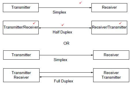
(4)
6.6.3 Half-duplex communication is when two devices take turns in communicating, one after the other.
Full-duplex communication is when two devices can both transmit and receive at the same time. (2)
6.7
6.7.1 A program is a sequence of instructions that tell a computer (PIC) how to do a task. (2)
6.7.2 A flow diagram is a visual representation of steps and decisions needed to perform and complete a process. (2)
6.8 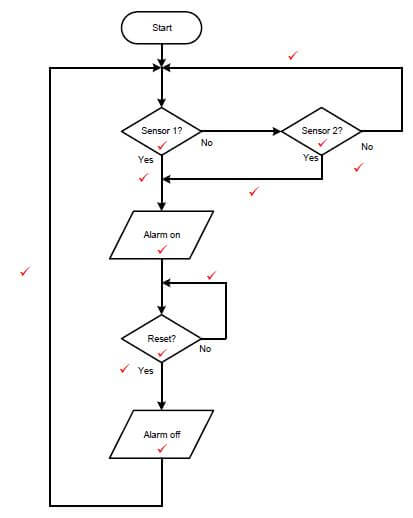
NOTE:
- 1 mark for each correct symbol (x 5)
- 1 mark for each correct placement of Yes/No (x 3)
- 1 mark for each correct flow line (x 4)
(12)
[50]
TOTAL: 200