ELECTRICAL TECHNOLOGY(DIGITAL) GRADE 12 QUESTIONS - NSC PAST PAPERS AND MEMOS NOVEMBER 2021
Share via Whatsapp Join our WhatsApp Group Join our Telegram GroupINSTRUCTIONS AND INFORMATION
- This question paper consists of SIX questions.
- Answer ALL the questions.
- Answer the following questions on the attached ANSWER SHEETS:
QUESTIONS 3.1.6, 3.5.2 and 3.6.2
QUESTION 4.1.2
QUESTIONS 5.3.2, 5.4 and 5.5.2
QUESTION 6.8 - Write your centre number and examination number on every ANSWER SHEET and hand them in with your ANSWER BOOK, whether you have used them or not.
- Sketches and diagrams must be large, neat and FULLY LABELLED.
- Show ALL calculations and round off answers correctly to TWO decimal places.
- Number the answers correctly according to the numbering system used in this question paper.
- You may use a non-programmable calculator.
- Calculations must include:
9.1 Formulae and manipulations where needed
9.2 Correct replacement of values
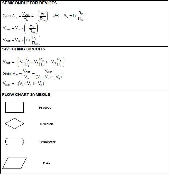
9.3 Correct answer and relevant units where applicable - A formula sheet is attached at the end of this question paper.
- Write neatly and legibly.
QUESTIONS
QUESTION 1: MULTIPLE-CHOICE QUESTIONS
Various options are provided as possible answers to the following questions. Choose the answer and write only the letter (A–D) next to the question numbers (1.1 to 1.15) in the ANSWER BOOK, e.g. 1.16 E.
1.1 Choose the correct example of an unsafe condition that is likely to cause damage to property or an injury:
- Running in the workshop
- Spilling liquid or oil without cleaning it up
- Faulty tools or equipment
- Overloading electrical outlets when connecting many appliances(1)
1.2 An astable multivibrator generates …
- one pulse cycle of high and low when a trigger pulse is applied.
- a continuous train of pulses without the need of a trigger pulse to be applied.
- one stable state without the trigger pulse being applied on its input.
- a sequence of triangular waveforms at the output.(1)
1.3 When applying a triangular waveform to the input of a differentiator, the output will be …
- a DC waveform.
- an inverted triangular waveform.
- a square waveform.
- the first harmonic wave of the triangular waveform.(1)
1.4 When the input voltage to a non-inverting Schmitt trigger is smaller than the reference voltage, the output is driven into ...
- positive saturation.
- negative saturation.
- both negative and positive saturation
- zero saturation. (1)
1.5 When a square wave is applied to the input of an op-amp integrator circuit, the output will be a …
- sine waveform.
- constant DC voltage.
- triangular waveform.
- square waveform. (1)
1.6 Pin 1 of an integrated circuit (IC) is indicated by …
- a white '1' on the IC.
- two blue lines on the IC.
- an indent with a dot on the left of the indent.
- the pin that is red in colour.(1)
1.7 The maximum current that a 555 IC can either sink or source:
- 2 A
- 200 A
- 2 mA
- 200 mA(1)
1.8 The light-altering principle that a liquid crystal display relies on is known as …
- polarisation.
- pixels.
- a matrix.
- back-lighting.(1)
1.9 A BCD decoder is a device that converts a binary code into a recognisable … form.
- octal
- hexadecimal
- decimal
- binary(1)
1.10 Counter circuits of which the flip-flops are not triggered at the same time are called …
- asynchronous.
- synchronous.
- pulse triggered.
- edge triggered.(1)
1.11 A register that loads the information one bit at a time and then moves the information out of the register in the same manner for each clock pulse applied is called the … register.
- Parallel-In: Parallel-Out
- Parallel-In: Serial-Out
- Serial-In: Parallel-Out
- Serial-In: Serial-Out(1)
1.12 The start-up instructions of a microcontroller is stored in the …
- ROM
- RAM
- CPU
- I/O unit (1)
1.13 A register that stores data that is needed as a part of any arithmetic operation is known as the …
- program counter.
- memory address register.
- accumulator.
- current instruction register. (1)
1.14 Identifying and removing errors in a program is called …
- looping.
- debugging.
- illegal data flow.
- an algorithm.(1)
1.15 One disadvantage of the inter-integrated bus (I2C) is that it …
- requires only two wires.
- is cheaper to implement.
- supports multiple master devices.
- has a slower speed.(1)
[15]
QUESTION 2: OCCUPATIONAL HEALTH AND SAFETY
2.1 State TWO functions of a health and safety representative. (2)
2.2 Give TWO examples of human rights in the workplace. (2)
2.3 Differentiate between an unsafe act and an unsafe condition. (2)
2.4 Risk analysis can be divided into different categories. Name ONE category. (1)
2.5 Define danger with reference to the Occupational Health and Safety Act, 1993 (Act 85 of 1993). (2)
2.6 Name ONE personal protective item you would use when etching a printed circuit board (PCB). (1)
[10]
QUESTION 3: SWITCHING CIRCUITS
3.1 Refer to FIGURE 3.1 below and answer the questions that follow.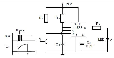
FIGURE 3.1: MONOSTABLE MULTIVIBRATOR
3.1.1 State the function of resistor R1. (2)
3.1.2 Write down the voltage across Pin 2 when switch S is pressed. (1)
3.1.3 State whether the LED will be ON or OFF when switch S is pressed. (1)
3.1.4 Determine the typical threshold voltage of the circuit. (1)
3.1.5 Explain why the switch bounce does not affect the output of the circuit. (2)
3.1.6 Draw the output on the ANSWER SHEET for QUESTION 3.1.6. (3)
3.2 Refer to FIGURE 3.2 below and answer the questions that follow.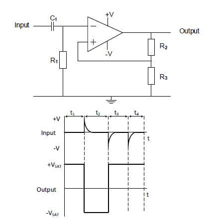
FIGURE 3.2: MULTIVIBRATOR
3.2.1 Identify the multivibrator circuit in FIGURE 3.2. (1)
3.2.2 State the function of resistor R2. (1)
3.2.3 Determine the polarity of the voltage on the non-inverting input during t1. (1)
3.2.4 Explain the operation of the circuit when a positive pulse is applied to the input. (4)
3.2.5 Explain why the output remains positive even after the pulse at t4 is applied. (2)
3.3 Refer to FIGURE 3.3 below and answer the questions that follow.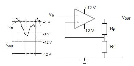
FIGURE 3.3: INVERTING SCHMITT TRIGGER
3.3.1 Identify the value of the trigger voltage levels. (2)
3.3.2 State how the trigger voltage level is determined. (1)
3.3.3 Explain whether the circuit uses open-loop or closed-loop gain. (2)
3.3.4 State TWO functions of the circuit. (2)
3.4 A summing amplifier consists of the following components:
| COMPONENT | DESCRIPTION |
| Dual supply | +12 V, 0 V, -12 V |
| 741 IC | Package (DIP 8) |
| R1 | 10 kΩ |
| R2 | 10 kΩ |
| R3 | 10 kΩ |
| RF | 100 kΩ |
NOTE: R1, R2 and R3 are input resistors. RF is a feedback resistor.
3.4.1 Draw the circuit diagram. (7)
3.4.2 Calculate output voltage if the following DC voltages are applied to the input resistors:
V1 = +0,5 V
V2 = -0,8 V
V3 = +0,2 V (3)
3.4.3 Explain how the polarity of the output will be affected if the input voltage V3 is increased to V3 = +0,4 V. (3)
3.5 Refer to FIGURE 3.5 below and answer the questions that follow.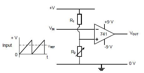
FIGURE 3.5: COMPARATOR
3.5.1 Name the components that determine the reference voltage. (2)
3.5.2 Draw the output voltage on the ANSWER SHEET for QUESTION 3.5.2. (3)
3.6 Refer to FIGURE 3.6 below and answer the questions that follow.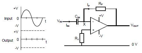
FIGURE 3.6: OP-AMP DIFFERENTIATOR
3.6.1 State TWO advantages of changing a passive differentiator to an active differentiator. (2)
3.6.2 Draw the output voltage on the ANSWER SHEET for QUESTION 3.6.2. (4)
[50]
QUESTION 4: SEMICONDUCTOR DEVICES
4.1 FIGURE 4.1 below shows an operational amplifier. Answer the questions that follow.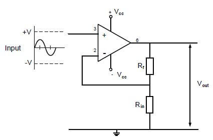
FIGURE 4.1: OPERATIONAL AMPLIFIER
4.1.1 Identify the type of operational amplifier in FIGURE 4.1. (1)
4.1.2 Draw the output voltage waveform on the ANSWER SHEET for QUESTION 4.1.2. (3)
4.1.3 Explain why operational amplifiers are known as differential voltage amplifiers. (1)
4.1.4 Give TWO reasons why negative feedback is important when the op amp is used as a linear amplifier. (2)
4.2 Refer to FIGURE 4.2 below and answer the questions that follow.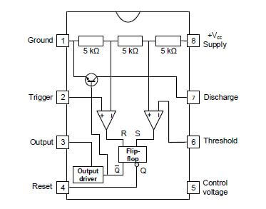
FIGURE 4.2: INTERNAL LAYOUT OF 555 TIMER IC
4.2.1 Explain the function of the RS flip-flop. (2)
4.2.2 State the typical operating voltage range of the 555 IC. (2)
4.2.3 Explain the function of the three 5 kΩ resistors inside the 555 IC. (2)
4.2.4 Name TWO modes of operation for the 555 IC. (2)
4.2.5 Explain the function of the threshold input on Pin 6 of a 555 IC. (2)
4.3 Refer to FIGURE 4.3 below and explain why the output is zero volts.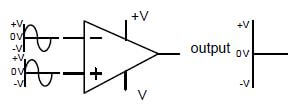
FIGURE 4.3: 741 OP AMP (3)
[20]
QUESTION 5: DIGITAL AND SEQUENTIAL DEVICES
5.1 Explain the term common cathode with reference to the seven-segment LED display. (2)
5.2 Draw a fully labelled circuit diagram of a sinking digital output. Indicate the direction of current flow at the output. (5)
5.3 Refer to FIGURE 5.3 below and answer the following questions.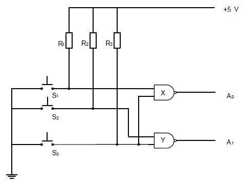
FIGURE 5.3: ENCODER
5.3.1 Explain the function of the encoder in FIGURE 5.3. (3)
5.3.2 Complete the logic state of inputs and outputs in boxes A to E on the ANSWER SHEET for QUESTION 5.3.2 when S1 is pressed. (5)
5.4 FIGURE 5.4 below represents the logic symbol of a flip-flop.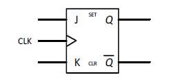
FIGURE 5.4: LOGIC SYMBOLOF A FLIP-FLOP
Draw the labelled logic circuit for the logic symbol in FIGURE 5.4 using AND gates and NOR gates only on the ANSWER SHEET for QUESTION 5.4. (9)
5.5 FIGURE 5.5 below represents the logic symbol of a half-adder. Answer the questions that follow.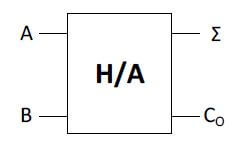
FIGURE 5.5: LOGIC SYMBOL OF A HALF-ADDER
5.5.1 Draw the logic circuit of a half-adder using an AND gate and an Exclusive-OR gate. (6)
5.5.2 Complete the truth table of the half-adder in the table (X, Y and Z) on the ANSWER SHEET for QUESTION 5.5.2.
| INPUTS | OUTPUTS | ||
| A | B | Σ | Co |
| 0 | 0 | 0 | 0 |
| 0 | 1 | X | 0 |
| 1 | 0 | 1 | Y |
| 1 | 1 | Z | 1 |
(3)
5.6 Name TWO applications of counters. (2)
5.7 Explain the difference between the full-sequence counter and the truncated counter. (2)
5.8 Explain the term positive edge triggering. (2)
5.9 Refer to FIGURE 5.9 below and explain the sequential operation of this counter without the aid of a truth table.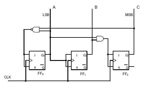
FIGURE 5.9: THREE-BIT SYNCHRONOUS SELF-STOPPING UP-COUNTER THAT STOPS AT 510 (1012) (8)
5.10 Draw a neatly labelled diagram of a four-bit serial-in: parallel-out shift register using D-type flip-flops. Show ALL the inputs and outputs. (8)
[55]
QUESTION 6: MICROCONTROLLERS
6.1 Define a microcontroller. (3)
6.2 Explain the principle of operation of a microcontroller. (4)
6.3 Answer the following questions with reference to the RS-232 communication protocol:
6.3.1 State the operating voltages for logic 1 and logic 0. (2)
6.3.2 Give TWO examples where the RS-232 can be used. (2)
6.4 Refer to FIGURE 6.4 below and answer the questions that follow.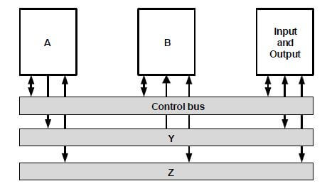
FIGURE 6.4: BLOCK DIAGRAM OF COMMUNICATION IN A MICROCONTROLLER
6.4.1 Label the following blocks in FIGURE 6.4:
- A (1)
- B (1)
6.4.2 Identify the following bus connections:
- Y (1)
- Z (1)
6.4.3 State the purpose of the control bus. (3)
6.5 Refer to FIGURE 6.5 below and answer the questions that follow.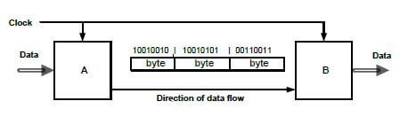
FIGURE 6.5: BLOCK DIAGRAM OF SERIAL DATA SYNCHRONOUS COMMUNICATION IN A MICROCONTROLLER
6.5.1 Label the following blocks in FIGURE 6.5:
- A (1)
- B (1)
6.5.2 Explain how data is transmitted from block A to block B in FIGURE 6.5. (6)
6.6 Answer the following questions with reference to communication in microcontrollers:
6.6.1 Define communication protocol in a microcontroller. (2)
6.6.2 Refer to FIGURE 6.6.2 of simplex communication below and show the difference between simplex communication and duplex communication by means of a neatly labelled block diagram.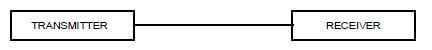
FIGURE 6.6.2: SIMPLEX COMMUNICATION (4)
6.6.3 Explain the difference between half-duplex communication and full-duplex communication. (2)
6.7 Define the following terms with reference to the software of microcontrollers:
6.7.1 Program (2)
6.7.2 Flow diagram (2)
6.8 Design a flow diagram of a home security system with TWO sensors. The first sensor is at the front door and the second sensor is at the window. If any of the sensors is activated, the alarm will be activated. Once the alarm has been reset, the sensors will continue monitoring the front door and the window. The alarm must include a reset function. NO timing function is required.
Complete and label the flow chart of this device on the ANSWER SHEET for QUESTION 6.8. (12)
[50]
TOTAL: 200
FORMULA SHEET
ANSWER SHEET
QUESTION 3: SWITCHING CIRCUITS
3.1.6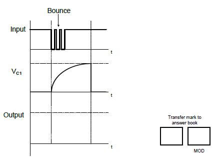
FIGURE 3.1.6 (3)
3.5.2
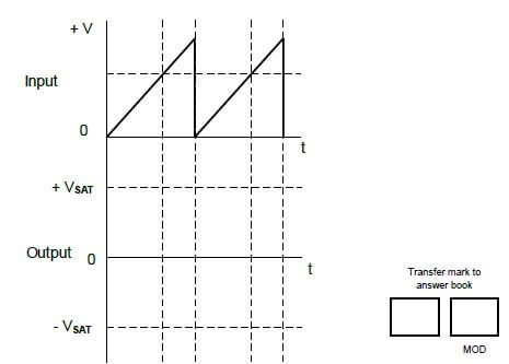
FIGURE 3.5.2 (3)
3.6.2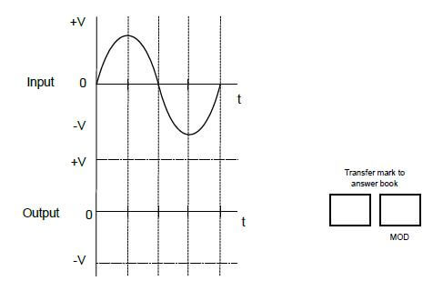
FIGURE 3.6.2 (4)
QUESTION 4: SEMICONDUCTOR DEVICES
4.1.2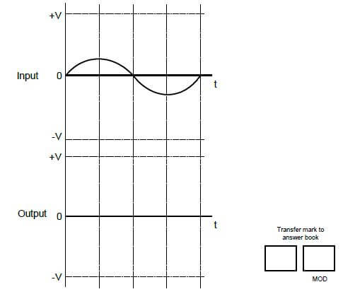
FIGURE 4.1.2 (2)
QUESTION 5: DIGITAL AND SEQUENTIAL DEVICES
5.3.2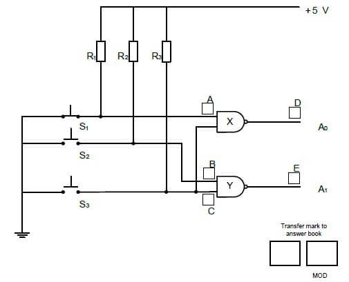
FIGURE 5.3.2 (5)
5.4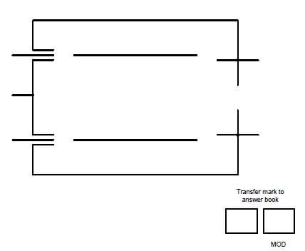
FIGURE 5.4 (9)
5.5.2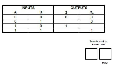
TABLE 5.5.2 (3)
QUESTION 6: MICROCONTROLLERS
6.8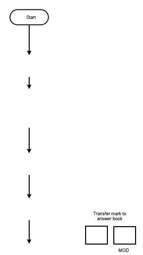
FIGURE 6.8 (12)