ELECTRICAL TECHNOLOGY (ELECTRONICS) GRADE 12 MEMORANDUM - NSC EXAMS PAST PAPERS AND MEMOS NOVEMBER 2020
Share via Whatsapp Join our WhatsApp Group Join our Telegram GroupELECTRICAL TECHNOLOGY: ELECTRONICS
GRADE 12
NOVEMBER 2020
MEMORANDUM
NATIONAL SENIOR CERTIFICATE
INSTRUCTIONS TO THE MARKERS
- All questions with multiple answers imply that any relevant, acceptable answer should be considered.
- Calculations:
2.1 All calculations must show the formulae.
2.2 Substitution of values must be done correctly.
2.3 All answers MUST contain the correct unit to be considered.
2.4 Alternative methods must be considered, provided that the correct answer is obtained.
2.5 Where an incorrect answer could be carried over to the next step, the first answer will be deemed incorrect. However, should the incorrect answer be carried over correctly, the marker has to re-calculate the values, using the incorrect answer from the first calculation. If correctly used, the candidate should receive the full marks for subsequent calculations. - These marking guidelines are only a guide with model answers. Alternative interpretations must be considered and marked on merit. However, this principle should be applied consistently throughout the marking session at ALL marking centres.
QUESTION 1: OCCUPATIONAL HEALTH AND SAFETY
1.1 Any article or part thereof which is manufactured, provided or installed ✓in the interest of the health or safety of any person.✓✓(2)
1.2 Your right to fair labour practices.✓✓
Your right to work reasonable hours.
Your right to belong to a trade union.
Your right to earn a living wage.
Your right not to be discriminated against. (1)
1.3
- If a person dies. ✓
- A major incident. ✓✓
- An incident where the health and safety of any person has been/was endangered. (2)
1.4
- To dismiss an employee without due process. ✓
- To reduce the rate of remuneration without due process. ✓
- Alter the terms of conditions of his/her employment to terms of conditions that is less favourable to him/herself. ✓
- Harassment and verbal abuse.
- Alter position relative to other people.
- Treat employees unfair because of race.
NOTE: If a learner only mentions an infringement of rights only 1 mark will be awarded. Duplicate mentioning of rights will not be awarded (3)
1.5 In an emergency it can be pushed and it would immediately cut all electric power ✓✓to all the equipment, stopping them,✓✓thus making the workshop safe.✓ (2)
[10]
QUESTION 2: RLC CIRCUITS
2.1
2.1.1 If VX lags VR by 35°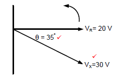
(2)
2.1.2 The voltages represent an RC circuit ✓ because, VR is always in phase with IT and VX lags VR by 35°. ✓
Because VR is in phase with IT and VX is lagging VR, thus proving that the circuit is predominantly capacitive as IT leads VX. (2)
2.2
2.2.1
XL = 2 x π x f x L
= 2 x π x 60 x 20 x 10-3
= 7,54 Ω (3)
OR
XL = VL
IT
XL = 49
6,5
XL = 7,54 Ω
2.2.2
VC = I x Xc
= 6.5 x 25
= 162,5 V (3)
2.2.3 The voltage is lagging, ✓ because the capacitive reactance is greater than the inductive reactance (VC is greater than VL). ✓(2)
2.2.4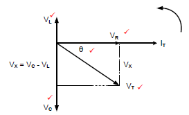
(5)
NOTE: 5 marks, 1 mark for each correct label of which VL, VC and VR are priority marks and thereafter any other two correct labels.
2.3 2.3.1 Phasor diagram of a parallel RLC✓ circuit at resonance. ✓ (2)
2.3.2 The voltage drop across the components in a parallel circuit is the same, ✓ hence the voltage is used as the reference. (1)
OR
The applied voltage is common across all components.
2.3.3 In a parallel resonant circuit impedance is at maximum, ✓ and the total current is at minimum. ✓ (2)
OR
The relationship between impedance and current in a parallel RLC circuit is inversely proportional.
2.4
2.4.1
fr = 1
2π√LC
= 1
2 x 3,142√300 x 10-3 x 150 x 10-6
= 23,73 Hz (3)
2.4.2
Q = 1/R x √L/C
= 1 x √300 x 10-3
20 150 x 10-6
= 2,24
(3)
OR
If candidates calculate XL or Xc they can use the following formulae:
XL = 2πfL
XL = 2π(23.73)(300 x 10-3)
XL = 44.73Ω
Q = XL/R
Q = 44.73
20
Q = 2,24
Q = XC/R
Q = 44.73
20
Q = 2,24
2.4.3
Z = 20Ω
Z = R at resonance (2)
2.4.4
C = 1
4 x π2 x L x fr2
= 1
4 x 9,87 x 300 x 10-3 x 4 x 106
= 2,111 x 10-8 F
= 21,11 nF (3)
OR
C = 1
(2πfr)2 x L
= 1
(2 x 3,14 x 2000)2 x 300 x 10-3
= 2,113 x 10-8 F
= 21,13 nF
For resonance. Calculating XL first and then since XL= XC
XL = 2πfL
XL = 2π(2000)(300 x 10-3)
= 3769.91Ω
C = 1
2πfXC
= 1
2π(2000)(3769.91)
= 21.11nF
2.5.
2.5.1 Q1 (1)
2.5.2 Reading the values from the graph where f1 = 30000 Hz and f2 = 35000 Hz the following can be deduced:
fr = f1 + f2
2
= 30000 + 35000
2
= 32500Hz
= 32,5 kHz (3)
NOTE: If the candidate deduced the value 32,5 kHz directly from the graph, full marks will be awarded.
Because the incorrect formula was provided on the formula sheet, the following calculation will be accepted.
fr = f1 + f2
2
= 35000 - 30000
2
= 2500Hz
2.5.3 Deducing the indicated bandwidth of Q1 from the graph as 35 kHz - 30 kHz the candidate will be able to calculate as follows:
BW = f - f
= 35000 - 30000
= 5000Hz
BW = fr
Q
Q = fr
BW
= 32500
5000
= 6,5
OR
BW = fr and BW=(f2 - f1)
Q
(f2 - f1) = fr
Q
Q = fr
(f2 - f1)
= 32500
(35000- 30000)
= 6,5 (3)
[40]
QUESTION 3: SEMICONDUCTOR DEVICES
3.1
3.1.1
- – Source ✓
- – Gate ✓
- – Drain ✓ (3)
3.1.2 N-type ✓ (1)
3.1.3 If the voltage on terminal B is 0 V, no current will flow between terminals A and C. ✓ (1)
3.1.4
A - Enhancement mode N-channel MOSFET ✓
C - P-channel JFET✓
E - Depletion mode P-channel MOSFET ✓ (3)
3.2 Negative resistance is a characteristic of the UJT when it is triggered on, the current through the emitter terminal of the UJT rises ✓ while its potential falls. ✓
Negative resistance is when the UJT is triggered 'on' current floods into the lower base region and as the resistance falls, current through the bar rises. At the same time, the potential on the emitter terminal is pulled down. (2)
3.3
3.3.1 The Darlington pair is able to deliver very high output currents✓ to drive a load from very small input base currents. ✓
Low output impedance to drive the output along long signal cable runs.
Very high input impedance in order to not pull / load down the preceding input stage. (2)
3.3.2 A BJT transistor normally needs 0,6 V to 0,7 V across its base emitter terminals to operate. ✓ The Darlington pair consists of two BJT transistors✓ who's base emitter terminals are connected in series, ✓therefore the Darlington pair will need a VBE voltage from 1,2 to 1,4 V to operate. (3)
3.4 3.4.1 Infinite open loop gain. ✓
Infinite input impedance. ✓
Zero output impedance.
Infinite bandwidth.
Common mode rejection ratio. (2)
3.4.2 The Op-amp is ideal for amplifying AC voltages because of its dual voltage supply ✓ which allows the output terminal to rise and fall above and below zero volts.✓ (2)
3.5 3.5.1 Point 'X' is known as virtual ground because both inputs have the same potential ✓ and the non-inverting input is connected to 0 V (ground) ✓ (2)
3.5.2
VOUT = VIN x (-RF/RIN)
RF = VOUT X RIN
VIN
= - 8 x 1.8 x 103
0.4
= 36 x 103 Ω
= 36 kΩ (3)
NOTE: The minus relates to the inverting function of the amplifier and is ignored for the resistive value of a resistor cannot be negative.
-36 kΩ is also accepted as correct.
3.6
3.6.1
Controlling the positioning of a servo device. ✓
Any timing application. (1)
3.6.2 Switch.✓ (1)
3.6.3 Comparator 1 compares the upper voltage set up by the three 5 kΩ resistors at ⅔ of the supply voltage ✓ to the threshold voltage on pin 6. ✓
Comparator 2 compares the lower voltage set up by the three 5 kΩ resistors at ⅓ of the supply voltage ✓ to the trigger voltage on pin 2. ✓ (4)
[30]
QUESTION 4: SWITCHING CIRCUITS
4.1 The astable multivibrator has no external trigger input.✓
The bistable multivibrator makes use of external trigger inputs. ✓ (2)
4.2
4.2.1 Astable multivibrator. (1)
4.2.2
- If point A is low it causes the Op-amp to saturate and its output to rise to +12 V. ✓
- This raises the potential across the voltage divider pair R1 and R2, making point B more positive than point A. ✓
- With the output voltage high, it induces the capacitor to charge towards +12 V through resistor RF, gradually increasing the voltage at point A. ✓
- When the voltage at point A becomes more positive than the voltage at point B, the Op-amp immediately saturates in the opposite direction with its output falling to -12 V. ✓
- This forces the capacitor to discharge (or charge towards -12 V) through resistor RF, decreasing the voltage at point A.✓
- When the voltage at point A falls below that of point B, the Op-amp saturates back to +12 V and the process repeats itself. ✓ (6)
4.2.3 The frequency of the multivibrator can be increased by either decreasing ✓ the value of RF or C1. ✓ (2)
4.3
4.3.1 Capacitor C2 removes any unwanted noise ✓ from the supply that might affect the timer operation✓ (2)
4.3.2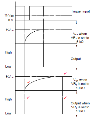
NOTE: 2 marks for the correct charging cycle of the capacitor 2 marks for the correct output signal. (4)
4.3.3 LED 2 will be ON ✓ because the output of the 555 IC goes high ✓ when the trigger switch is pressed, forward biasing LED 2✓ and reverse biasing LED 1. (3)
4.4
4.4.1 This is a closed loop mode ✓ Op-amp circuit because RF creates a positive feedback loop from the output to the non-inverting input. ✓ (2)
4.4.2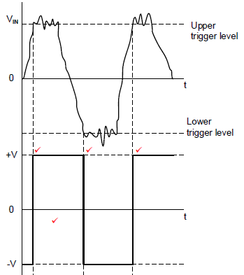
NOTE: 1 mark for each correct trigger point.
1 mark for the correct orientation. (4)
4.4.3 The trigger voltage levels can be adjusted by changing ✓ the value of either RF ✓ or R1. (2)
4.5 4.5.1 Coupling capacitor✓ used to pass the desired AC signals from the input and block unwanted DC signals. (1)
4.5.2
VOUT = -(V1 x RF x V2 x RF)
R1 R2
= -(0.5 x 10000 + 0.2 x 10000)
2000 500
= -6,5 V (3)
4.5.3 This amplifier is connected to a dual or split supply. ✓ The +12 V supply allows for the amplification of all positive signals ✓ and the -12 V supply allows for the amplification of all negative signals. ✓ (3)
4.5.4 If switch S1 is open, the output voltage will decrease, ✓ because input V1 is disconnected and will not be added and only V2 will be reflected on the output. ✓ (2)
4.6
4.6.1 Inverting ✓ comparator. ✓ (2)
4.6.2 
NOTE: 1 mark for each correct trigger point.
1 mark for correct orientation. (4)
4.6.3 The Op-amp is used in open loop mode therefore; ✓ there is no feedback loop to limit the gain of the Op-amp, ✓ driving it into saturation. (2)
4.7
- When the square wave input rises, both plates of the capacitor initially rises to the voltage of the square wave input. ✓
- As the left hand plate is held high, while the right-hand plate discharges through resistor R. ✓
- When the square wave falls to zero, the capacitor cannot discharge instantly, ✓ so both its plates follow the input voltage, instantly falling, with the left plate at zero and the right plate forced down to a value more negative than its initial charge.✓
- The right-hand plate then discharges, falling to zero. ✓ (5)
4.8
4.8.1
- On applying a square wave to the integrator input, the input voltage immediately rises to a steady positive value. ✓
- The input resistor then has a fixed voltage on the one end and a virtual ground 0 V at its other end.✓
- According to Ohm's law, this will cause a fixed current to flow, ✓ which is fed via the virtual ground point to the capacitor, charging it at a rate of R x C = t. ✓
- As the Op-amp's inputs are both at 0 V, it holds the left-hand plate of the capacitor at 0 V, ✓causing the right-hand plate to steadily fall in voltage. ✓ In line with the discharging characteristics of a capacitor. (6)
4.8.2
(2)
NOTE: 1 mark for inversion
1 mark tops and bottoms being clipped
Due to this being an active op-amp integrator, and not a passive circuit the following response will also be considered:
4.8.3
(2)
[60]
QUESTION 5: AMPLIFIERS
5.1 5.1.1 Feedback is defined as a process whereby a part of the output signal ✓ is fed back to the input stage.✓ (2)
5.1.2 Distortion is defined as a condition that will occur when the amplification is no longer linear✓ in form or frequency. ✓ (2)
Distortion is an undesired change of a signal passing from the input to the output stage of an amplifier circuit.
NOTE: If frequency is not mentioned, but the learner demonstrates the understanding of additional factors causing distortion or the alteration of the wave shape, the second mark will be awarded.
5.2
5.2.1 RC coupled Amplifier. ✓
Common Emitter Amplifier. (1)
5.2.2 The emitter-base junction (EB) must be forward biased above the cutoff region✓ and below the saturation region.✓ The collector-base junction (CB) must be reversed biased ✓ for the transistor to operate in the Active region for amplification to take place✓
OR
The values of resistors R1 and R2 must be chosen so that the Q point of the transistor is biased in the middle of the load line allowing for 360° of the input signal to be amplified. (4)
5.2.3
VRC = VCC - VCE
= 9 - 2,38
= 6,62V(3)
OR
VCC = VCE + (IC x RC)
9 = 2.38 + (IC x 470)
IC = 14.09mA
VRC = IC x RC
VRC = 14.09 x 10-3 x 470
VRC = 6.62V
For the alternative method marks will be awarded as follows:
1 mark for the first calculation
2 marks for the correct final calculation
NOTE: VRE is included in the value of VCE as shown in the data on the circuit diagram.
In the case of a learner indicating that he cannot calculate VRC due to VRE not being indicated separately on the diagram, 3 marks will be awarded.
In the case of no answer, 0 marks.
5.2.4
AV = 20 log VOUT
VIN
= 20 log 2.38
2 x 10-3
= 61,51 dB (3)
5.2.5 When VIN increases then VBE will increase above the Q point ✓ and T1 is switched on harder. ✓ The internal resistance of T1 is reduced due to an increased base current. ✓ IC increase and VCE reduces due to lower resistance of T1 and increase in IC. The result is reduction in output voltage and 180° phase shift. ✓ The gain of a transistor is fixed. (5)
5.3
- = Base current (IB) ✓
- = Base-emitter voltage (VBE) ✓
- = Input Voltage ✓ OR change in VBE (ΔVBE) (3)
5.4
5.4.1 Push-Pull Amplifier. ✓ (1)
5.4.2 NPN transistor. ✓ (1)
5.4.3 Each transistor is biased for Class B (180°) amplification✓ when no signal is applied to the input transformer, no alternating signal is applied to the base of Q1 and Q2. Because the Q point is so low, no current will flow in the circuit. ✓ (3)
5.4.4
- The input transformer has a centre-tapped secondary which acts as a splitter to produce two equal ✓and opposite signals during each half-cycle.✓
- Transistors Q1 and Q2 conduct when its base becomes positive with respect to its emitters✓ each amplifying the alternate half input signal.
- The centre-tapped output transformer combines the two half-cycles to produce one complete cycle. ✓ (Class A result)
- Each transistor conducts for alternate half-cycles only. ✓ (Class B amplification) (5)
5.5
5.5.1 Class C amplification. ✓ (1)
5.5.2 Radio Frequency (RF) amplifiers are narrow band amplifiers ✓ capable of amplifying only the band of frequencies ✓which is the information carrier and suppresses all other frequencies. ✓ (3)
5.5.3 The resonating frequency of the circuit can be varied by adjusting the value of the variable capacitors. ✓ (1)
5.5.4 Band pass filter. ✓ (1)
5.5.5 Energy transfer in the tank circuit is achieved when the tank circuit oscillates at the resonant frequency. ✓ When the amplifier receives an input signal which is amplified via T1, this amplified audio signal is modulated onto the resonant radio frequency of the tank circuit.✓ The result is a mixed output signal that includes the resonant radio frequency of the tank circuit as well as the modulated audio signal. ✓ (3)
5.6
5.6.1 Hartley Oscillator. ✓ (1)
5.6.2
- When first switched ON, the collector voltage rises and allows the capacitor in the tank circuit to charge. ✓
- The voltage drop across the inductors is in an inverted form, driving the transistor's base in the opposite direction thereby switching it OFF. ✓
- The capacitor will discharge through the inductors and push the tank circuit into oscillation. ✓
- During oscillation the voltages at each end of the tank circuit are 180° out of phase with each other, relative to their 0 V common centre tap point. ✓
- This ensures that the collector voltage is 180° out of phase with the base voltage. ✓
- The freewheeling effect of the tank circuit's operation then begins to drive the transistor alternately ON and OFF which in turn continually re-charges the tank circuit keeping it oscillating at a constant amplitude. ✓ (6)
5.6.3 Feedback in the circuit is obtained with the signal being fed back from the collector terminal of Q1 ✓ through capacitor C1 that is connected to the resonating tank circuit ✓ which are 180° out of phase with each other ✓ and then through capacitor C2 to the base of transistor Q1. Q1 is in common emitter configuration which creates another 180° phase shift. ✓ (4)
5.6.4 Inductor L3 is a RF choke used to prevent ✓ the AC resonant signal from being fed back to the base via R1 at 180° phase shift through the DC supply✓ which will cause the oscillations to fade away quickly. ✓ (3)
5.7 The FET will minimise the loading effect ✓ on preceding stages, as it has a higher input impedance when compared to the relatively low input impedance of the Bipolar Junction transistor (BJT). ✓ (2)
5.8
- They both produce a pure sinusoidal output waveform✓
- They both use positive feedback✓
- They both use a tank circuit for oscillation.
- They both use a transistor for amplification. (2)
[60]
TOTAL: 200