ELECTRICAL TECHNOLOGY (ELECTRONICS) GRADE 12 QUESTIONS - NSC EXAMS PAST PAPERS AND MEMOS NOVEMBER 2020
Share via Whatsapp Join our WhatsApp Group Join our Telegram GroupELECTRICAL TECHNOLOGY: ELECTRONICS
GRADE 12
NOVEMBER 2020
NATIONAL SENIOR CERTIFICATE
INSTRUCTIONS AND INFORMATION
- This question paper consists of FIVE questions.
- Answer ALL the questions.
- Answer QUESTIONS 2.3.2, 2.4.2, 2.6.2, 2.8.2, 2.8.3, 4.4, 4.5, 4.8.1, 4.8.2, 4.11.1 and 5.10 on the attached ANSWER SHEETS.
- Write your CENTRE NUMBER and EXAMINATION NUMBER on every ANSWER SHEET and staple them to your ANSWER BOOK, whether you have used them or not.
- Sketches and diagrams must be large, neat and FULLY LABELLED.
- Show ALL calculations and round off answers correctly to TWO decimal places.
- Number the answers correctly according to the numbering system used in this question paper.
- You may use a non-programmable calculator.
- Calculations must include:
9.1 Formulae and manipulations where needed
9.2 Correct replacement of values
9.3 Correct answers and relevant units where applicable - A formula sheet is attached at the end of this question paper.
- Write neatly and legibly.
QUESTION 1: OCCUPATIONAL HEALTH AND SAFETY
1.1 Define health and safety equipment. (2)
1.2 Name ONE human right in the workplace. (1)
1.3 Name TWO incidents that should be reported to inspectors at the workplace. (2)
1.4 State THREE types of victimisation by an employer that are forbidden. (3)
1.5 Describe how the master switch in a workshop contributes to safety. (2)
[10]
QUESTION 2: RLC CIRCUITS
2.1 Two AC voltages, VR and VX, each have maximum values of VR = 20 V and VX = 30 V respectively.
2.1.1 Draw the phasor diagram (NOT to scale) on the ANSWER SHEET for QUESTION 2.1.1 if VX lags VR by 35°. (2)
2.1.2 Explain whether the voltages represent an RL circuit or an RC circuit. (2)
2.2 The RLC series circuit in FIGURE 2.2 below consists of a resistor of 15 Ω, an inductance of 20 mH and a capacitive reactance of 25 Ω. The components are all connected in series across a 150 V/60 Hz AC supply. Answer the questions that follow.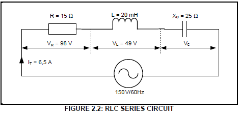
Given:
R = 15 Ω
L = 20 mH
XC = 25 Ω
VT = 150 V
f = 6 0 H z
IT = 6,5 A
2.2.1 Calculate the inductive reactance of the inductor. (3)
2.2.2 Calculate the voltage drop across the capacitor. (3)
2.2.3 Indicate whether the supply voltage is lagging or leading. Motivate your answer. (2)
2.2.4 Draw the phasor diagram of the circuit on the ANSWER SHEET for QUESTION 2.2.4. (5)
2.3 Refer to FIGURE 2.3 below and answer the questions that follow.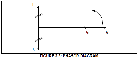
2.3.1 Identify the phasor diagram in FIGURE 2.3. (2)
2.3.2 State why the supply voltage is used as the reference in the phasor diagram. (1)
2.3.3 Explain the relationship between the total current and the impedance in a parallel resonant circuit. (2)
2.4 Refer to FIGURE 2.4 below and answer the questions that follow.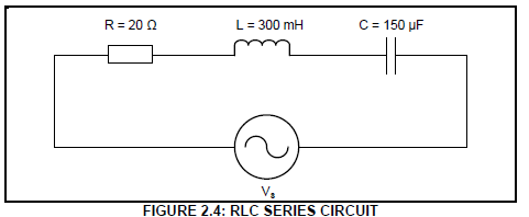
Given:
R = 20 Ω
L = 300 mH
C = 150 μF
2.4.1 Calculate the resonant frequency. (3)
2.4.2 Calculate the quality factor of the circuit. (3)
2.4.3 Determine the impedance of the circuit at resonance. Motivate your answer. (2)
2.4.4 Calculate the value of the capacitance required for the circuit in FIGURE 2.4 to resonate at 2 kHz. (3)
2.5 FIGURE 2.5 below shows the Q-factor characteristic curve of an RLC circuit, NOT to scale. Q1, Q2 and Q3 indicate how a change in the L/C ratio affects the Q-factor of a resonant circuit. Answer the questions that follow.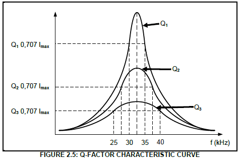
2.5.1 Identify the curve with the highest selectivity. (1)
2.5.2 Calculate the resonant frequency for response curve Q1. (3)
2.5.3 Calculate the quality factor for Q1. (3)
[40]
QUESTION 3: SEMICONDUCTOR DEVICES
3.1 FIGURE 3.1 below shows a cross-section of the construction of an enhancement mode MOSFET. Answer the questions that follow.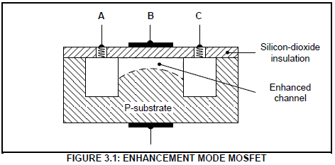
3.1.1 Identify A, B and C. (3)
3.1.2 Indicate whether the enhanced channel consists of P-type or N-type material. (1)
3.1.3 State what will happen to the current between terminal A and terminal C if the voltage on terminal B is 0 V. (1)
3.1.4 FIGURE 3.1.4 below shows the various FET symbols. Identify the components represented by symbols A, C and E.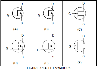
3.2 Explain the term negative resistance with reference to the UJT. (2)
3.3 Refer to FIGURE 3.3 below and answer the questions that follow.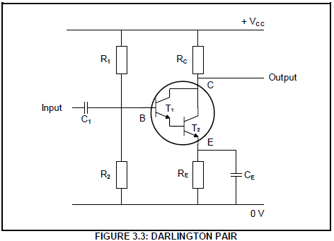
3.3.1 Explain why the Darlington pair is preferred to a single transistor for this circuit. (2)
3.3.2 Explain why the Darlington pair needs a minimum of 1,2 V to 1,4 V across its base-emitter terminals to operate. (3)
3.4 Refer to FIGURE 3.4 below and answer the questions that follow.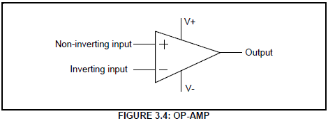
3.4.1 Name TWO characteristics of an ideal op-amp. (2)
3.4.2 Explain what makes the op-amp ideal to amplify alternating voltages. (2)
3.5 FIGURE 3.5 below shows the circuit diagram of an inverting op amp.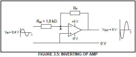
3.5.1 Explain why point X on the diagram is also known as the virtual ground. (2)
3.5.2 Calculate the value of feedback resistor RF. (3)
3.6 FIGURE 3.6 below shows the internal circuit diagram of a 555 IC. Answer the questions that follow.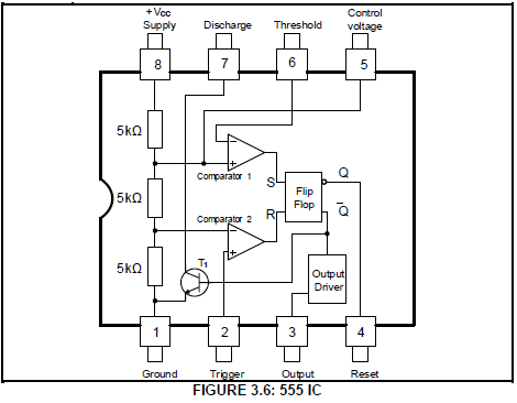
3.6.1 State ONE industrial application where the 555 IC is used as a timing device. (1)
3.6.2 Indicate whether transistor T1 acts as a switch or as an amplifier in the circuit. (1)
3.6.3 Explain the function of the two comparators in FIGURE 3.6. (4)
[30]
QUESTION 4: SWITCHING CIRCUITS
4.1 State ONE distinct difference between the astable multivibrator and the bistable multivibrator with reference to their inputs. (2)
4.2 Refer to FIGURE 4.2 below and answer the questions that follow.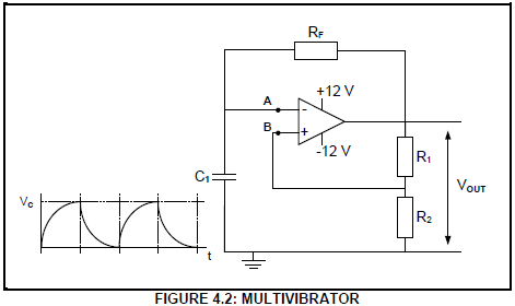
4.2.1 Identify the multivibrator in FIGURE 4.2. (1)
4.2.2 Describe the operation of the multivibrator in FIGURE 4.2 from a point where the capacitor has just discharged and point A is low. (6)
4.2.3 Explain how the frequency of the multivibrator in FIGURE 4.2 can be increased. (2)
4.3 FIGURE 4.3 below shows a monostable multivibrator using a 555 IC.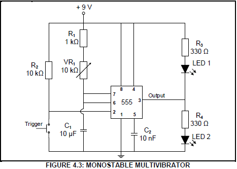
4.3.1 State the function of capacitor C2. (2)
4.3.2 FIGURE 4.3.2 below shows the trigger input, capacitor charge and output signals of the multivibrator in FIGURE 4.3. The variable resistor (VR1) is set to 5 kΩ. On the ANSWER SHEET for QUESTION 4.3.2, draw the charging voltage VC1 and corresponding output if variable resistor (VR1) is changed to 10 kΩ.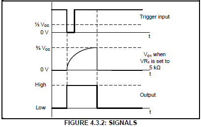
4.3.3 State whether LED 1 or LED 2 will be ON after the trigger switch is pressed. Motivate your answer. (3)
4.4 FIGURE 4.4 below shows the circuit diagram of a non-inverting Schmitt trigger. Answer the questions that follow.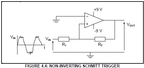
4.4.1 Indicate whether this is an open-loop mode op-amp circuit or a closed-loop mode op-amp circuit. Motivate your answer. (2)
4.4.2 Draw the output waveform of the Schmitt trigger on the ANSWER SHEET for QUESTION 4.4.2. (4)
4.4.3 State how the trigger voltage levels of the Schmitt trigger can be adjusted without changing the supply voltage. (2)
4.5 Refer to FIGURE 4.5 below and answer the questions that follow.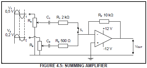
4.5.1 State the function of capacitor C1. (1)
4.5.2 Calculate the value of the output voltage. (3)
4.5.3 Explain what makes it possible for this amplifier to amplify both positive and negative voltages. (3)
4.5.4 Explain how the output voltage will be affected if switch S1 is open. (2)
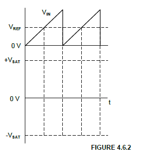
4.6 Refer to FIGURE 4.6 below and answer the questions that follow.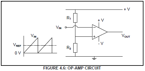
4.6.1 Identify the op-amp circuit in FIGURE 4.6. (2)
4.6.2 Draw the output signal of the op amp on the ANSWER SHEET for QUESTION 4.6.2. (4)
4.6.3 Explain why this op-amp circuit is driven into saturation during its operation. (2)
4.7 Explain the operation of the passive RC differentiator in FIGURE 4.7 below.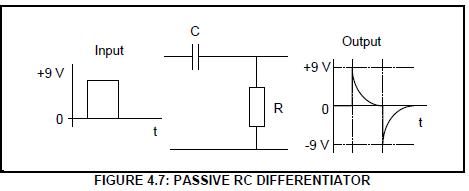
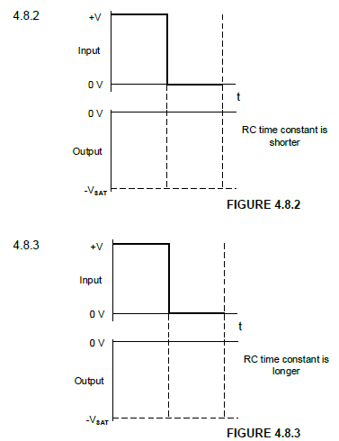
4.8 FIGURE 4.8 below shows an op-amp integrator with input and output signals.
Answer the questions that follow.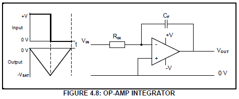
4.8.1 Explain why the op-amp integrator is able to produce a steadily falling output voltage when a square wave is applied to the input. (6)
4.8.2 On the ANSWER SHEET for QUESTION 4.8.2, draw the output waveform of the op-amp when the RC time constant is shortened from the given state. (2)
4.8.3 On the ANSWER SHEET for QUESTION 4.8.3, draw the output waveform of the op-amp when the RC time constant is lengthened from the given state. (2)
[60]
QUESTION 5: AMPLIFIERS
5.1 Define the following terms with reference to amplifiers:
5.1.1 Feedback (2)
5.1.2 Distortion (2)
5.2 Refer to FIGURE 5.2 below and answer the questions that follow.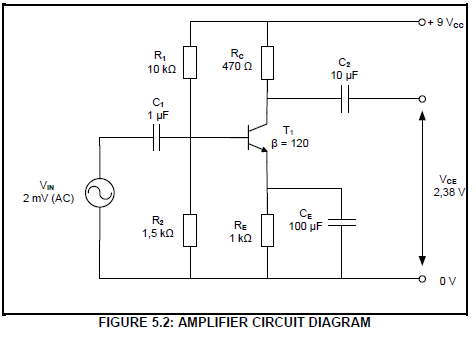
5.2.1 Identify the amplifier in FIGURE 5.2. (1)
5.2.2 Describe the biasing method for Class A amplification. (4)
5.2.3 Determine the voltage drop across RC. (3)
5.2.4 Calculate the voltage gain of the circuit in decibels. (3)
5.2.5 Explain how an increase in VIN will affect the output voltage (VCE) of the amplifier in FIGURE 5.2. (5)
5.3 FIGURE 5.3 below shows the input characteristic curve of a common emitter amplifier. Identify A, B and C.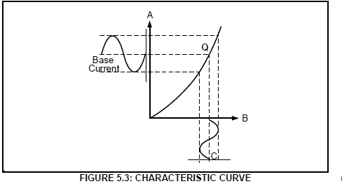
5.4 Refer to FIGURE 5.4 below and answer the questions that follow.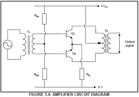
5.4.1 Identify the amplifier circuit in FIGURE 5.4. (1)
5.4.2 Identify the type of transistor used in the circuit. (1)
5.4.3 Explain why the circuit in FIGURE 5.4 will not consume power when the input signal is zero. (3)
5.4.4 Discuss the principle of operation of the amplifier in FIGURE 5.4. (5)
5.5 Refer to the LC resonant circuit of a radio-frequency amplifier and its input characteristics in FIGURE 5.5 below and answer the questions that follow.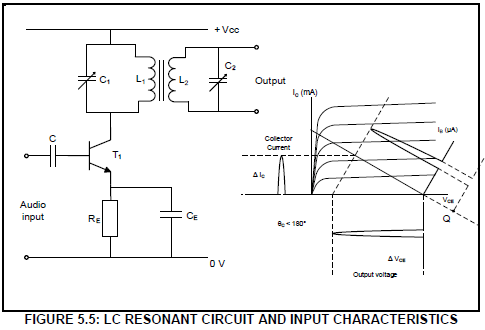
5.5.1 Name the class of amplification used by the circuit in FIGURE 5.5. (1)
5.5.2 Describe a radio-frequency amplifier. (3)
5.5.3 Indicate how the resonating frequency of the circuit in FIGURE 5.5 can be varied. (1)
5.5.4 Name the filter which blocks all frequencies, except those between certain limits. (1)
5.5.5 Explain energy transfer in the tank circuit which allows the RF amplifier to execute its function. (3)
5.6 Refer to FIGURE 5.6 below and answer the questions that follow.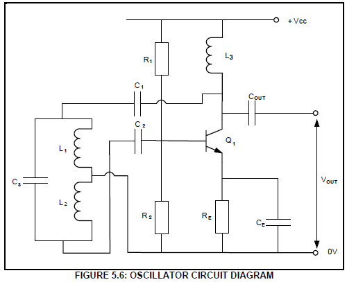
5.6.1 Identify the oscillator in FIGURE 5.6. (1)
5.6.2 Discuss how oscillation is achieved in this circuit. (6)
5.6.3 Describe how feedback is obtained in the circuit. (4)
5.6.4 Explain the function of inductor L3. (3)
5.7 Explain why a field-effect transistor (FET) is preferred over a bipolar junction transistor (BJT) in oscillator circuits. (2)
5.8 State TWO similarities between the Colpitts oscillator and the Hartley oscillator. (2)
[60]
TOTAL: 200
FORMULA SHEET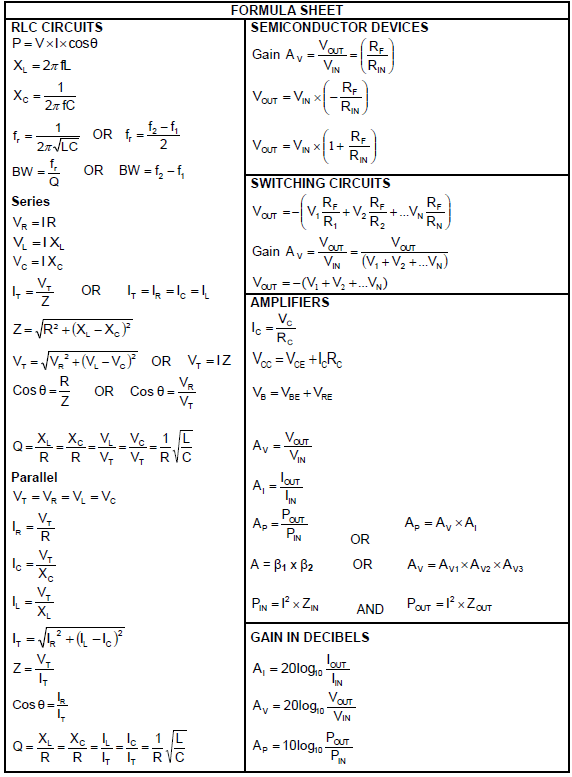
QUESTION 2: RLC CIRCUITS
QUESTION 4: SWITCHING CIRCUITS
4.3.2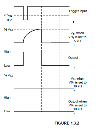
4.4.2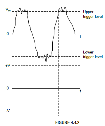
4.6.2 VIN