ELECTRICAL TECHNOLOGY (DIGITAL) GRADE 12 MEMORANDUM - NSC EXAMS PAST PAPERS AND MEMOS NOVEMBER 2020
Share via Whatsapp Join our WhatsApp Group Join our Telegram GroupELECTRICAL TECHNOLOGY: DIGITAL
GRADE 12
NOVEMBER 2020
MEMORANDUM
NATIONAL SENIOR CERTIFICATE
INSTRUCTIONS TO THE MARKERS
- All questions with multiple answers imply that any relevant, acceptable answer should be considered.
- Calculations:
2.1 All calculations must show the formulae.
2.2 Substitution of values must be done correctly.
2.3 All answers MUST contain the correct unit to be considered.
2.4 Alternative methods must be considered, provided that the correct answer is obtained.
2.5 Where an incorrect answer could be carried over to the next step, the first answer will be deemed incorrect. However, should the incorrect answer be carried over correctly, the marker has to re-calculate the values, using the incorrect answer from the first calculation. If correctly used, the candidate should receive the full marks for subsequent calculations. - These marking guidelines are only a guide with model answers. Alternative interpretations must be considered and marked on merit. However, this principle should be applied consistently throughout the marking session at ALL marking centres.
QUESTION 1: OCCUPATIONAL HEALTH AND SAFETY
1.1 Any article or part thereof which is manufactured, provided or installed ✓in the interest of the health or safety of any person.✓✓(2)
1.2 Your right to fair labour practices.✓✓
Your right to work reasonable hours.
Your right to belong to a trade union.
Your right to earn a living wage.
Your right not to be discriminated against. (1)
1.3
- If a person dies. ✓
- A major incident. ✓✓
- An incident where the health and safety of any person has been/was endangered. (2)
1.4
- To dismiss an employee without due process. ✓
- To reduce the rate of remuneration without due process. ✓
- Alter the terms of conditions of his/her employment to terms of conditions that is less favourable to him/herself. ✓
- Harassment and verbal abuse.
- Alter position relative to other people.
- Treat employees unfair because of race.
NOTE: If a learner only mentions an infringement of rights only 1 mark will be awarded. Duplicate mentioning of rights will not be awarded (3)
1.5 In an emergency it can be pushed and it would immediately cut all electric power ✓✓to all the equipment, stopping them,✓✓thus making the workshop safe.✓ (2)
[10]
QUESTION 2: SWITCHING CIRCUITS
2.1 The astable multivibrator has no external trigger input. ✓
The bistable multivibrator makes use of external trigger inputs. ✓ (2)
2.2
2.2.1 Astable multivibrator✓ (1)
2.2.2
- If point A is low it causes the Op-amp to saturate and its output to rise to +12 V. ✓
- This raises the potential across the voltage divider pair R1 and R2, making point B more positive than point A. ✓
- With the output voltage high, it induces the capacitor to charge towards +12 V through resistor RF, gradually lifting the voltage at point A. ✓
- When the voltage at point A becomes more positive than the voltage at point B, the Op-amp immediately saturates in the opposite direction with its output falling to -12 V. ✓
- This forces the capacitor to discharge (or charge towards -12 V) through resistor RF, lowering the voltage at point A. ✓
- When the voltage at point A falls below that of point B, the Op-amp saturates back to +12 V and the process repeats itself.✓ (6)
OR - The capacitor, C1 starts to charge up from the output voltage, (Vout) through feedback resistor, (RF) at a rate determined by their RC time constant.
- The capacitor will charge up fully to the value of Vout which is +Vsat.
- When the capacitor charging voltage at point “A” is equal to or greater than the voltage at point point “B”, the output will change state and be driven to the opposing negative supply rail.
- The voltage across the capacitor plates is now negative –Vsat.
- This sudden reversal of the output voltage causes the capacitor to discharge until point A is low again the process will repeat.
2.2.3 The frequency of the multivibrator can be increased by either decreasing ✓ the value of RF or C. ✓ (2)
2.3 2.3.1 Capacitor C2 removes any unwanted noise ✓ from the supply that might affect the timer operation. ✓ (2)
2.3.2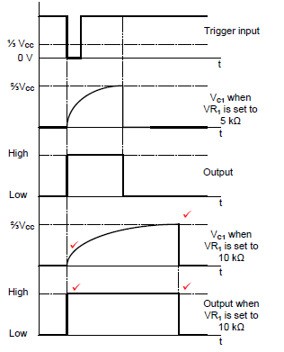
NOTE: 2 marks for the correct charging cycle of the capacitor 2 marks for the correct output signal. (4)
2.3.3 LED 2 will be ON ✓ because the output of the 555 IC goes high ✓ when the trigger switch is pressed, forward biasing ✓LED 2 and reverse biasing LED 1. (3)
2.4 2.4.1 This is a closed loop mode ✓ Op-amp circuit because RF creates a positive feedback loop from the output to the non-inverting input. ✓ (2)
2.4.2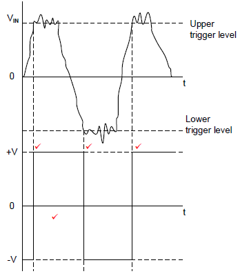
NOTE: 1 mark for each correct trigger point.
1 mark for the correct orientation. (4)
2.4.3 The trigger voltage levels can be adjusted by changing the value✓ of either RF or R1.✓
NOTE: 2 marks for mentioning one (2)
2.5
2.5.1 Coupling capacitor used to pass the desired AC signals from the input and block unwanted DC signals. (1)
2.5.2
VOUT = -(V1 x RF + V2 x RF )
R1 R2
=-(0.5 x 10000 + 0.2 x 10000)
2000 500
= -6,5 V (3)
2.5.3 This amplifier is connected to a dual or split supply. ✓ The +12 V supply allows for the amplification of all positive signals✓ and the -12 V supply allows for the amplification of all negative signals. ✓ (3)
2.5.4 If switch S1 is open, the output voltage will decrease, ✓ because input V1 is disconnected and will not be added and only V2 will be reflected on the output.✓ (2)
2.6 2.6.1 Inverting ✓ comparator. ✓ (2)
2.6.2 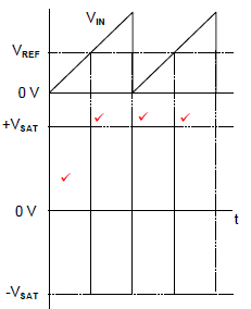
NOTE: 1 mark for each correct trigger point.
1 mark for correct orientation. (4)
2.6.3 The op-amp is used in open loop mode therefore; ✓ there is no feedback loop to limit the gain of the op-amp, ✓ driving it into saturation. (2)
2.7
- When the square wave input rises, both plates of the capacitor initially rises to the voltage of the square wave input. ✓
- As the left hand plate is held high, while the right-hand plate discharges through resistor R. ✓
- When the square wave falls to zero, the capacitor cannot discharge instantly, ✓ so both its plates follow the input voltage, instantly falling, with the left plate at zero and the right plate forced down to a value more negative than its initial charge. ✓
- The right-hand plate then discharges, falling to zero. ✓ (5)
OR - When the initial positive-going edge of the input signal is applied to the capacitor, it “appears” as a short circuit.
- After the initial positive-going edge of the input signal has passed and the peak value of the input is constant, the capacitor starts to charge up in its normal way via the resistor.
- As the capacitor charges up, the voltage across the resistor, decreases in an exponential way until the capacitor becomes fully charged resulting in a zero output across the resistor.
- Thus the voltage across the fully charged capacitor equals the value of the input pulse as: VC = VIN.
- The input pulse returns to zero, and the capacitor starts to discharge.
- After the initial negative-going edge of the input signal, the output voltage across the resistor, starts to increase exponentially.
2.8
2.8.1
- On applying a square wave to the integrator input, the input voltage immediately rises to a steady positive value. ✓
- The input resistor then has a fixed voltage on the one end and a virtual ground 0 V at its other end. ✓
- According to Ohm's law, this will cause a fixed current to flow, ✓which is fed via the virtual ground point to the capacitor, charging it at a rate of R x C = t. ✓
- As the Op-amp's inputs are both at 0 V, it holds the left-hand plate of the capacitor at 0 V, ✓causing the right-hand plate to steadily fall in voltage. ✓ In line with the discharging characteristics of a capacitor. (6)
2.8.2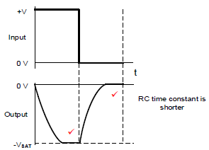
(2)
NOTE: 1 mark for inversion
1 mark tops and bottoms being clipped Due to this being an active op-amp integrator, and not a passive circuit the following response will also be considered: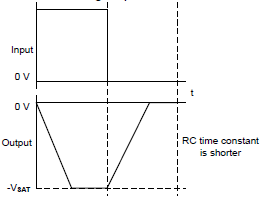
2.8.3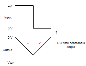
(2)
[60]
QUESTION 3: SEMICONDUCTOR DEVICES
3.1 3.1.1 Infinite open loop gain. ✓
Infinite input impedance. ✓
Zero output impedance. ✓
Infinite bandwidth.
Common mode rejection ratio.
NOTE: The following answers are incorrectly mentioned in the textbook as characteristics of an 'Ideal Op-Amp' and should also be considered.
Wide bandwidth
High input impedance
Low output impedance (3)
3.1.2 The Op-amp is ideal for amplifying AC voltages because of its dual voltage supply ✓ which allows the output terminal to rise and fall above and below zero volts. ✓ (2)
3.2 3.2.1 Point “X” is known as virtual ground because both inputs have the same potential ✓ and the non-inverting input is connected to 0 V (ground) ✓ (2)
3.2.2
VOUT = VIN x (- RF)
RIN
RF = -VOUT x RIN
VIN
= - 8 x 1.8 x 103
0.4
= 36 x 103 Ω
= 36kΩ (3)
NOTE: The minus relates to the inverting function of the amplifier and is ignored for the resistive value of a resistor cannot be negative. -36 kΩ is also accepted as correct.
3.3 3.3.1 Controlling the positioning of a servo device. ✓
Any timing application. (1)
3.3.2 Astable mode ✓ (1)
3.3.3 Switch. ✓ (1)
3.3.4 Comparator 1 compares the upper voltage set up by the three 5 kΩ resistors at ⅔ of the supply voltage✓ to the threshold voltage on pin 6. ✓
Comparator 2 compares the lower voltage set up by the three 5 kΩ resistors at ⅓ of the supply voltage✓ to the trigger voltage on pin 2. ✓ (4)
3.3.5 The flip-flop
- activates the output driver,✓
- switches transistor T1 on ✓
- and resets the IC. ✓ (3)
[20]
QUESTION 4: DIGITAL AND SEQUENTIAL DEVICES
4.1 Common Anode✓
Common Cathode ✓ (2)
4.2 Sourcing✓digital output (1)
4.3 Pulse triggered ✓ (master/slave)
Edge triggered✓
NOTE: If a learner wrote positive edge triggered or negative edge triggered, marks must be awarded. (2)
4.4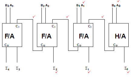
(8)
4.5
| INPUTS | OUTPUTS | ||||
| A | B | 0 | 1 | 2 | 3 |
| 0 | 0 | 1 | 0 | 0 | 0 |
| 0 | 1 | 0 | 1 | 0 | 0 |
| 1 | 1 | 0 | 0 | 0 | 1 |
(8)
4.6 A decoder converts a binary code ✓into a recognisable decimal form, ✓ either as a digit or a character. (2)
4.7 Combinational logic circuits✓
Sequential logic circuits✓ (2)
4.8
4.8.1
| MODE OF OPERATION | INPUTS | OUTPUTS | ||
| S | R | Q | Q ̅ | |
| HOLD | 0 | 0 | No change | |
| RESET | 0 | 1 | 0 | 1 |
| SET | 1 | 0 | 1 | 0 |
| ILLEGAL | 1 | 1 | X | X |
| INVALID | ||||
(4)
OR
| MODE OF OPERATION | INPUTS | OUTPUTS | ||
| S | R | Q | Q ̅ | |
| ILLEGAL | 0 | 0 | 0 | 0 |
| SET | 0 | 1 | 1 | 0 |
| RESET | 1 | 0 | 0 | 1 |
| HOLD | 1 | 1 | No change | |
4.8.2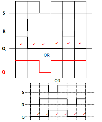
(6)
NOTE: If SET and RESET are both “1” the principle of NO CHANGE for the inputs at both 1's should be followed.
4.9 A counter is a circuit which counts through a set sequence of states (numbers)✓ when activated by a clock pulse,✓ and once counted it returns to its original state✓ (3)
4.10 Propagation delay is where the timing signal is delayed ✓ through each flipflop.(2)
OR
NOTE: If the learner only responds with a drawing as shown below, 1 mark will be awarded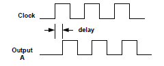
4.11
4.11.1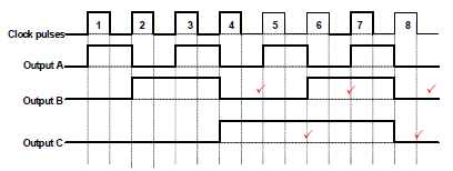
(5)
4.11.2 The purpose of the AND gate is to prevent FF2 from producing an incorrect reading on the second clock pulse ✓ when FF0 and FF1 are both high (310 or 112) ✓and the next pulse must produce a 410 (1002).✓ (3)
OR
The purpose of the AND gate is to ensure that inputs J and K of FF2 are only high when both Q0 and Q1 are at logic '1' (that is, at a count of 310 or 112). It is only when these two outputs are high that the next clock pulse (the fourth) toggle FF2 output Q2 high to logic '1'. At this pulse Q0 and Q1 naturally toggle low to logic '0', resulting in the circuit producing an output count of 1002 or 410, with output Q2 being the most-significant-bit (1002 = 410).
4.12 4.12.1 Parallel-in-parallel-out ✓shift register (1)
4.12.2
- = 4-bit parallel data input ✓
- = 4-bit parallel data output ✓ (2)
4.12.3
- Data is introduced at input A in a parallel format ✓
- Data is then transferred through to the output pins by the same clock pulse✓
- One clock pulse loads ✓ and unloads the register. ✓ (4)
[55]
QUESTION 5: MICROCONTROLLERS
5.1
- Lighting, in advertising and illumination of spaces ✓
- Stock control ✓
- Refrigeration control (2)
5.2
5.2.1
- = ROM✓
- = RAM ✓
If answers are swopped, full marks must be awarded. (2)
5.2.2 The CPU is responsible for interpreting✓ and executing the stored instructions✓ from the ROM programme. ✓ (3)
5.2.3 The Input/Output unit enables the microcontroller to communicate ✓with the outside world✓via peripherals. ✓ (3)
5.3 Products based on microcontrollers can be smaller and cheaper. ✓
Products based on microcontrollers can have fewer components and are more reliable.✓
Product assembly is simpler, quicker and cheaper✓
Product using microcontrollers are more flexible because their features are programmed into the chip and not build into the hardware. (3)
5.4 5.4.1 A CPU register (processor register) is one of a small set of data holding places✓ that are part of the computer processor.✓ (2)
5.4.2
- Programme Counter (PC) ✓
- Memory Address Register (MAR) ✓
- Memory Data Register (MDR) ✓
- Current Instruction Register (CIR) (3)
5.5
5.5.1 An analogue to digital converter converts an analogue signal into its digital equivalent. ✓ (2)
5.5.2 A/D converters are used in microcontrollers to detect an analogue signal and convert it to a digital format which the CPU can interpret.✓ (2)
5.6
5.6.1 A = Data bus ✓ (1)
5.6.2 The control bus is used mainly for the CPU to issue control instructions ✓to both memory as well as input/output ports. ✓ (2)
5.6.3 The address bus is used to transmit the memory addresses ✓from the memory and input/output ports to the CPU. ✓ (2)
5.7
5.7.1 SPI is a synchronous serial communication data link✓ that operates in full duplex (signals carrying data in both directions simultaneously).✓ It uses separate clock and data lines as well as a select line✓to choose the device chosen to receive data. (3)
5.7.2 The function of the SPI is to send data between microcontrollers and small peripherals. ✓ (1)
5.7.3 Digital signal processors ✓
Shift Registers ✓
Sensors (2)
5.8
5.8.1 Logic '1' = -200mV ✓ or less
Logic '0' = +200mV ✓ or more
NOTE: This values can change from one device to another. (2)
OR
Logic „0‟ = any answer less than -200mV
Logic „1‟= any answer more than +200mV
5.8.2
- Point of sale terminals ✓
- Metering instruments ✓
- PLC's ✓
- CNC machines
- Robots
- Embedded control computers
- Medical instruments (3)
5.9
5.9.1
- = Sender/Transmitter ✓
- = Direction of data flow ✓/data flow
- = Receiver ✓ (3)
5.9.2
- Data is sent as one long stream of bits, or as a block of data.✓
- At the receiving end, the bits are counted and reconstructed into bytes.✓
- Strict timing between the transmitter and receiver units is essential.✓
- Both the sender and receiver are synchronised with a common clock pulse sent to both the transmitter and receiver. ✓ (4)
5.10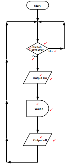
NOTE: 1 mark for each correct shape (4)
Decision = 3 marks
Output on = 1mark
Output off = 1mark
Timer = 1 mark
Start = 1 mark
Total marks MUST not exceed 10 marks. (10)
[55]
TOTAL: 200