ELECTRICAL TECHNOLOGY (DIGITAL) GRADE 12 QUESTIONS - NSC EXAMS PAST PAPERS AND MEMOS NOVEMBER 2020
Share via Whatsapp Join our WhatsApp Group Join our Telegram GroupELECTRICAL TECHNOLOGY: DIGITAL
GRADE 12
NOVEMBER 2020
NATIONAL SENIOR CERTIFICATE
INSTRUCTIONS AND INFORMATION
- This question paper consists of FIVE questions.
- Answer ALL the questions.
- Answer QUESTIONS 2.3.2, 2.4.2, 2.6.2, 2.8.2, 2.8.3, 4.4, 4.5, 4.8.1, 4.8.2, 4.11.1 and 5.10 on the attached ANSWER SHEETS.
- Write your CENTRE NUMBER and EXAMINATION NUMBER on every ANSWER SHEET and staple them to your ANSWER BOOK, whether you have used them or not.
- Sketches and diagrams must be large, neat and FULLY LABELLED.
- Show ALL calculations and round off answers correctly to TWO decimal places.
- Number the answers correctly according to the numbering system used in this question paper.
- You may use a non-programmable calculator.
- Calculations must include:
9.1 Formulae and manipulations where needed
9.2 Correct replacement of values
9.3 Correct answers and relevant units where applicable - A formula sheet is attached at the end of this question paper.
- Write neatly and legibly.
QUESTION 1: OCCUPATIONAL HEALTH AND SAFETY
1.1 Define health and safety equipment. (2)
1.2 Name ONE human right in the workplace. (1)
1.3 Name TWO incidents that should be reported to inspectors at the workplace. (2)
1.4 State THREE types of victimisation by an employer that are forbidden. (3)
1.5 Describe how the master switch in a workshop contributes to safety. (2)
[10]
QUESTION 2: SWITCHING CIRCUITS
2.1 State ONE distinct difference between the astable multivibrator and the bistable multivibrator with reference to their inputs. (2)
2.2 Refer to FIGURE 2.2 below and answer the questions that follow.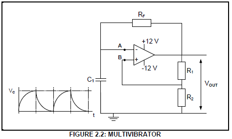
2.2.1 Identify the multivibrator in FIGURE 2.2. (1)
2.2.2 Describe the operation of the multivibrator in FIGURE 2.2 from a point where the capacitor has just discharged and point A is low. (6)
2.2.3 Explain how the frequency of the multivibrator in FIGURE 2.2 can be increased. (2)
2.3 FIGURE 2.3 below shows a monostable multivibrator using a 555 IC.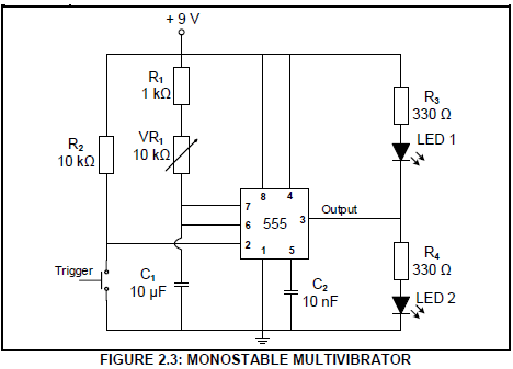
2.3.1 State the function of capacitor C2. (2)
2.3.2 FIGURE 2.3.2 below shows the trigger input, capacitor charge and output signals of the multivibrator in FIGURE 2.3. The variable resistor (VR1) is set to 5 kΩ. On the ANSWER SHEET for QUESTION 2.3.2, draw the charging voltage VC1 and corresponding output if variable resistor (VR1) is changed to 10 kΩ. (4)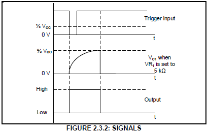
2.3.3 State whether LED 1 or LED 2 will be ON after the trigger switch is pressed. Motivate your answer. (3)
2.4 FIGURE 2.4 below shows the circuit diagram of a non-inverting Schmitt trigger. Answer the questions that follow.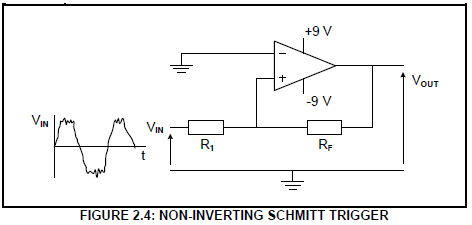
2.4.1 Indicate whether this is an open-loop mode op-amp circuit or a closed-loop mode op-amp circuit. Motivate your answer. (2)
2.4.2 Draw the output waveform of the Schmitt trigger on the ANSWER SHEET for QUESTION 2.4.2. (4)
2.4.3 State how the trigger voltage levels of the Schmitt trigger can be adjusted without changing the supply voltage. (2)
2.5 Refer to FIGURE 2.5 below and answer the questions that follow.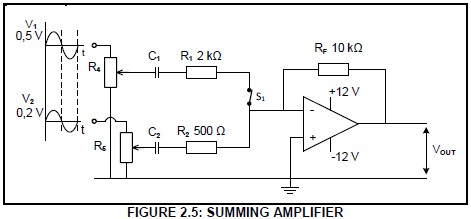
2.5.1 State the function of capacitor C1. (1)
2.5.2 Calculate the value of the output voltage. (3)
2.5.3 Explain what makes it possible for this amplifier to amplify both positive and negative voltages. (3)
2.5.4 Explain how the output voltage will be affected if switch S1 is open. (2)
2.6 Refer to FIGURE 2.6 below and answer the questions that follow.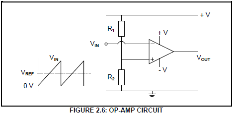
2.6.1 Identify the op-amp circuit in FIGURE 2.6. (2)
2.6.2 Draw the output signal of the op amp on the ANSWER SHEET for QUESTION 2.6.2. (4)
2.6.3 Explain why this op-amp circuit is driven into saturation during its operation. (2)
2.7 Explain the operation of the passive RC differentiator in FIGURE 2.7 below.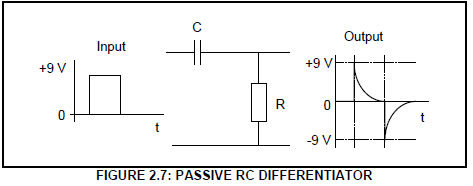
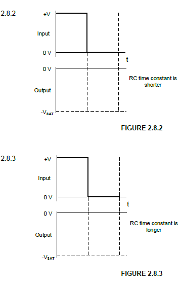
2.8 FIGURE 2.8 below shows an op-amp integrator with input and output signals.
Answer the questions that follow.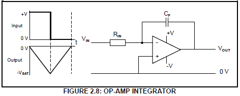
2.8.1 Explain why the op-amp integrator is able to produce a steadily falling output voltage when a square wave is applied to the input. (6)
2.8.2 On the ANSWER SHEET for QUESTION 2.8.2, draw the output waveform of the op amp when the RC time constant is shortened from the given state. (2)
2.8.3 On the ANSWER SHEET for QUESTION 2.8.3, draw the output waveform of the op-amp when the RC time constant is lengthened from the given state. (2)
[60]
QUESTION 3: SEMICONDUCTOR DEVICES
3.1 Refer to FIGURE 3.1 below and answer the questions that follow.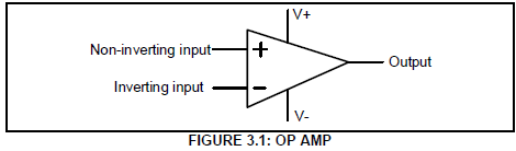
3.1.1 Name THREE characteristics of an ideal op amp. (3)
3.1.2 Explain what makes the op-amp ideal to amplify alternating voltages. (2)
3.2 FIGURE 3.2 below shows the circuit diagram of an inverting op-amp.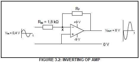
3.2.1 Explain why point X on the diagram is also known as the virtual ground. (2)
3.2.2 Calculate the value of feedback resistor RF. (3)
3.3 FIGURE 3.3 below shows the internal circuit diagram of a 555 IC. Answer the questions that follow.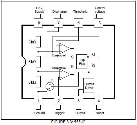
3.3.1 State ONE industrial application where the 555 IC is used as a timing device. (1)
3.3.2 Name the mode in which the 555 IC will operate to produce a musical note. (1)
3.3.3 Indicate whether transistor T1 acts as a switch or as an amplifier in the circuit. (1)
3.3.4 Explain the function of the two comparators in FIGURE 3.3. (4)
3.3.5 Explain the function of the flip-flop in FIGURE 3.3. (3)
[20]
QUESTION 4: DIGITAL AND SEQUENTIAL DEVICES
4.1 Name TWO methods to connect the LEDs of an LED seven-segment display to the supply. (2)
4.2 Identify the circuit in FIGURE 4.2 below with reference to digital outputs. (1)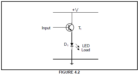
4.3 With reference to the triggering of flip-flops, name the TWO classes of synchronous flip-flops. (2)
4.4 FIGURE 4.4 below represents an incomplete block diagram of a 4-bit parallel adder. Complete and label the diagram of this adder on the ANSWER SHEET for QUESTION 4.4. (8)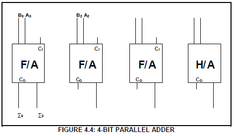
4.5 FIGURE 4.5 below represents the circuit diagram of a binary-to-decimal decoder. Complete the truth table of this decoder on the ANSWER SHEET for QUESTION 4.5. (8)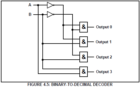
| INPUTS | OUTPUTS | ||||
| A | B | 0 | 1 | 2 | 3 |
| 0 | 0 | 1 | 0 | 0 | 0 |
| 0 | 1 | ||||
| 1 | 1 | ||||
4.6 State the function of a decoder. (2)
4.7 Name TWO group classifications of logic circuits with reference to memory elements. (2)
4.8 Refer to FIGURE 4.8 below and answer the questions that follow.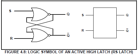
4.8.1 Complete the truth table of the RS latch on the ANSWER SHEET for QUESTION 4.8.1. (4)
| MODE OF OPERATION | INPUTS | OUTPUTS | ||
| S | R | Q | Q | |
| ILLEGAL | 0 | 0 | ||
| SET | 0 | 1 | 0 | |
| RESET | 1 | 0 | 0 | |
| HOLD | 1 | 1 | NoChange | |
4.8.2 Complete the output waveforms of this RS latch on the ANSWER SHEET for QUESTION 4.8.2. (6)
4.9 Explain the term counter. (3)
4.10 Explain the term propagation delay with reference to asynchronous ripple counters. (2)
4.11 FIGURE 4.11 below shows the circuit diagram of a three-stage synchronous binary counter.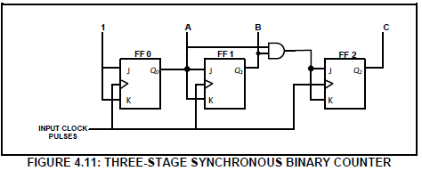
4.11.1 Complete the output waveforms of this counter on the ANSWER SHEET for QUESTION 4.11.1. (5)
4.11.2 Explain the purpose of the AND gate in FIGURE 4.11. (3)
4.12 Refer to FIGURE 4.12 below and answer the questions that follow.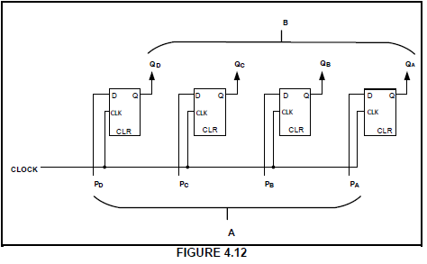
4.12.1 Identify the register in FIGURE 4.12. (1)
4.12.2 Label A and B. (2)
4.12.3 Describe the operation of this register. (4)
[55]
QUESTION 5: MICROCONTROLLERS
5.1 State TWO applications of microcontrollers in commercial devices. (2)
5.2 Refer to FIGURE 5.2 below and answer the questions that follow.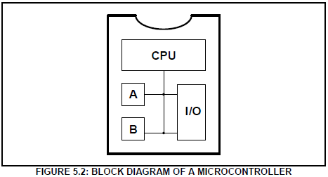
5.2.1 Identify A and B. (2)
5.2.2 Describe the function of the CPU. (3)
5.2.3 Describe the function of the input/output unit (I/O). (3)
5.3 List THREE advantages of microcontrollers over traditional discrete electronic components. (3)
5.4 With reference to the registers of a CPU:
5.4.1 Describe the CPU register. (2)
5.4.2 List THREE special purpose registers. (3)
5.5 Refer to FIGURE 5.5 below and answer the questions that follow.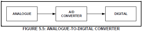
5.5.1 Explain the function of the A/D converter. (2)
5.5.2 Explain why an A/D converter is used with microcontrollers. (2)
5.6 Refer to FIGURE 5.6 below and answer the questions that follow.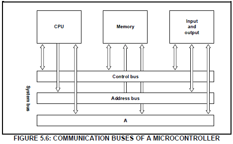
5.6.1 Label A. (1)
5.6.2 Explain the function of the control bus. (2)
5.6.3 Explain the function of the address bus. (2)
5.7 With reference to serial peripheral interfaces (SPI):
5.7.1 State the characteristics of the serial peripheral interface (SPI). (3)
5.7.2 State the function of the serial peripheral interface (SPI). (1)
5.7.3 State TWO applications of the serial peripheral interface (SPI). (2)
5.8 Answer the following questions with reference to the RS-485 communication protocol.
5.8.1 State the typical operating voltages for logic '1' and logic '0'. (2)
5.8.2 List THREE devices that can be used with the RS-485 interface. (3)
5.9 Refer to FIGURE 5.9 below and answer the questions that follow.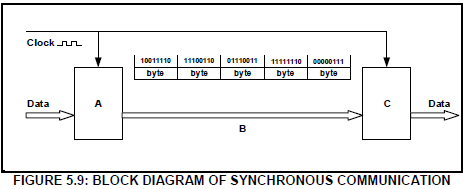
5.9.1 Label A, B and C. (3)
5.9.2 Describe how data is transferred through the device. (4)
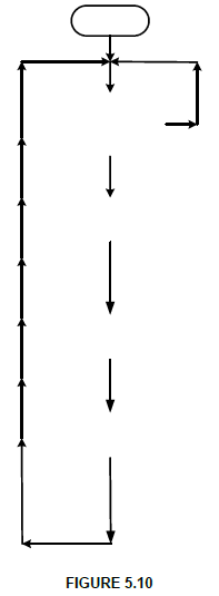
5.10 Design a flow chart for a monostable device which has only ONE stable state. It changes state when it is triggered by an input, and stays in that state for 5 seconds. It then returns to its original state.
Complete and label the flow chart for this device on the ANSWER SHEET for QUESTION 5.10. (10)
[55]
TOTAL: 200
FORMULA SHEET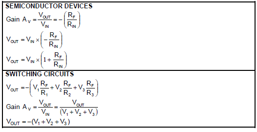
QUESTION 2: SWITCHING CIRCUITS
2.3.2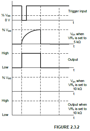
2.4.2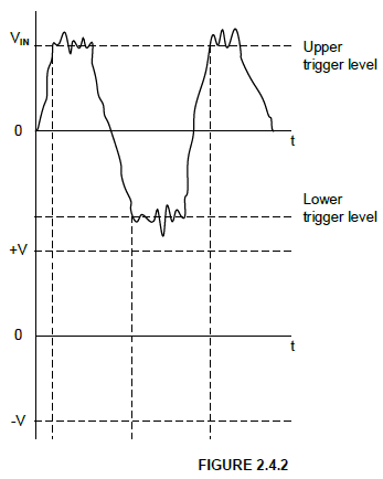
2.6.2 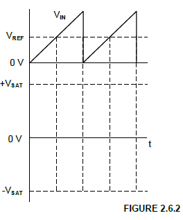
QUESTION 4: DIGITAL AND SEQUENTIAL DEVICES
4.4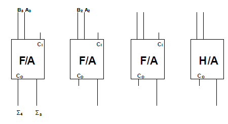 (8)
(8)
4.8.2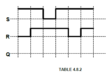
4.11.1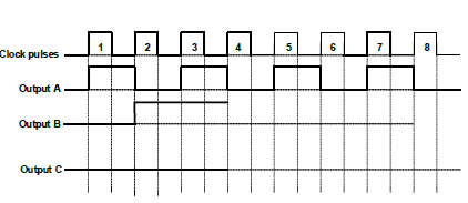
5.10