Electrical Technology: Digital Electronics Questions - Grade 12 September 2021 Preparatory Exams
Share via Whatsapp Join our WhatsApp Group Join our Telegram GroupINSTRUCTIONS AND INFORMATION
- This question paper consists of SIX questions.
- Sketches and diagrams must be large, neat and FULLY LABELLED.
- Show ALL calculations and round off answers to TWO decimal places.
- Number the answers correctly according to the numbering system used in this question paper.
- Answer the following questions on the attached ANSWER SHEETS:
QUESTION 5.2.1
QUESTION 5.2.2
QUESTION 5.3.2
QUESTION 5.5 - You may use a non-programmable calculator.
- Show the units for ALL answers of calculations.
- A formula sheet is provided at the end of this question paper.
- Write neatly and legible.
QUESTIONS
QUESTION 1: MULTIPLE CHOICE QUESTIONS
Various options are given as possible answers to the following questions. Choose the answer and write only the letter (A–D) next to the question numbers (1.1 to 1.15) in the ANSWER BOOK, for example 1.16 A
1.1 To prevent infection when treating burns the following should NOT be done:
- Do not take a pain killer
- Do not pop blisters
- Do not use a sterile gauze or bandage
- Do not hold the burned area under cool running water (1)
1.2 With reference to a monostable multivibrator, the time an output stays high is determined by:
- The time constant (RC)
- The length of time you push the button
- The magnitude of the supply voltage
- It will stay high indefinitely (1)
1.3 The Bistable multivibrator has the following characteristics:
- Free running with ONE input
- Free running with TWO inputs
- TWO stable states with TWO inputs
- NO stable states with ONE input (1)
1.4 A Light Dependant Resistor (LDR) will change value due to:
- Wind blowing on the LDR
- Current flowing through the LDR
- A voltage drop across the LDR
- The change of light shining on the LDR (1)
1.5 The output waveform of a Schmitt trigger circuit will always be a:
- Sine wave
- Triangular wave
- Radio wave
- Square wave (1)
1.6 Pin 1 of an Integrated Circuit (IC) is indicated by the following:
- A white ‘1’ on the IC
- Two blue lines on the IC
- An indent with a dot to the left of the indent
- The pin is red in colour (1)
1.7 The maximum current a 555 IC can either sink or source is:
- 2 A
- 200 A
- 2 Ma
- 20 Ma (1)
1.8 With reference to the LED seven segment display, common anode refers to:
- The anodes of all eight LED’s are connected together to a common ground rail.
- The cathodes of all eight LED’s are connected together to a common positive rail.
- The anodes of all eight LED’s are connected together to a common positive rail.
- None of the above. (1)
1.9 The function of a decoder is to …
- convert analogue signal to a digital signal.
- convert a digital signal to an analogue signal.
- convert a binary code into a recognisable decimal form.
- convert a decimal code into a recognisable binary form. (1)
1.10 Pulse triggered flip-flop circuits are also referred to as:
- Master/Slave
- Follow my lead
- Simultaneous trigger
- Continuous trigger (1)
1.11 The term ‘full sequence counter’ refers to:
- A counter that counts from 0 to 5
- A counter that runs to its maximum count
- A counter that is interrupted during the count
- A counter that stops counting at 2 (1)
1.12 With reference to microcontrollers, a … is an example of an input.
- sensors
- motors
- monitors
- LED display (1)
1.13 The term ‘CPU’ refers to:
- Common Programming Unit
- Central Programming Unit
- Central Processing Unit
- Common Processing Unit (1)
1.14 The term ‘Debugging’ refers to:
- To identify and remove errors
- To find bugs and kill them
- To find bugs and remove them
- All of the above (1)
1.15 The Inter-Integrated Bus (I2C) is an official standard serial communication protocol that requires only …
- 4 lines.
- 3 lines.
- 1 line.
- 2 lines. (1)
[15]
QUESTION 2: OCCUPATIONAL HEALTH AND SAFETY
2.1 Give the meaning of the following with reference to the Occupational Health and Safety, 1993 (Act 85 of 1993).
2.1.1 Risk (1)
2.1.2 Safe (1)
2.2 Explain the difference between quantitative risk analysis and qualitative risk analysis. (5)
2.3 State ONE example of a dangerous practice in an electrical workshop. (1)
2.4 Explain how inadequate lighting is an unsafe condition. (2) [10]
QUESTION 3: SWITCHING CIRCUITS
3.1 With reference to FIGURE 3.1 below, answer the following questions.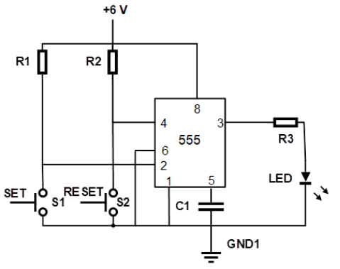
FIGURE 3.1: MULTIVIBRATOR
3.1.1 Identify the circuit in FIGURE 3.1 above. (1)
3.1.2 State the function of R3. (1)
3.1.3 Describe what happens when the RESET switch, S2 is pressed. (3)
3.1.4 Explain the purpose of C1 which is connected to ground from pin 5. (3)
3.1.5 Explain what the effect would be on the circuit if R1 and R2 were not added to the circuit. (2)
3.2 Draw a fully labelled circuit diagram for a monostable multivibrator op-amp circuit. (6)
3.3 Explain how you would vary the length of time that a monostable multivibrator circuit output stays ‘HIGH’. (3)
3.4 Explain how to eliminate switch bounce. (1)
3.5 Draw a fully labelled circuit diagram for a temperature sensor using a 741 op-amp. (8)
3.6 Explain the principle of operation of a Light Dependant Resistor (LDR). (4)
3.7 Refer to FIGURE 3.7 below and answer the questions that follow.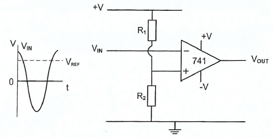
FIGURE 3.7: COMPARATOR
3.7.1 Explain what is meant with open loop with reference to FIGURE 3.7. (2)
3.7.2 Describe the principles of operation of a comparator. (6)
3.8 Refer to FIGURE 3.8 below and answer the questions that follow.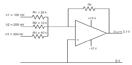
FIGURE 3.8: SUMMING AMPLIFIER
3.8.1 State how an input signal can be added to the summing amplifier. (1)
3.8.2 Calculate the value of the feedback resistor (RF). (4)
3.8.3 State why the output voltage is negative in FIGURE 3.8. (1)
3.9 Draw the circuit diagram for a passive integrator. (4)
[50]
QUESTION 4: SEMICONDUCTOR DEVICES
4.1 Name the THREE stages of an op-amp. (3)
4.2 Identify Pin 7 of a 741 op-amp. (1)
4.3 With reference to op-amp characteristics, explain the term bandwidth. (4)
4.4 Explain why an op-amp as a voltage follower is an ideal coupling stage (buffer) between two unevenly matched stages. (2)
4.5 With reference to 555 IC, explain the function of pin 5 (control voltage). (4)
4.6 Explain the function of using a small value capacitor connected from pin 5 to ground on a 555 IC. (2)
4.7 Name the TWO primary building blocks of a 555 IC. (2)
4.8 Name TWO modes the 555 IC is set up to function in. (2)
[20]
QUESTION 5: DIGITAL AND SEQUENTIAL DEVICES
5.1 Refer to the LED seven-segment display and explain the difference between a common anode and a common cathode.
(4)
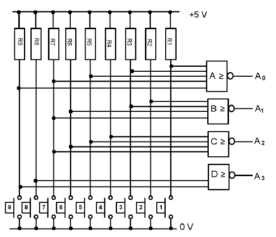
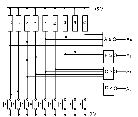
5.2 Refer to FIGURE 5.2 below and determine the binary code at the output when the following input switches are pressed. Write the answers on ANSWER SHEETS 5.2.1 and 5.2.2.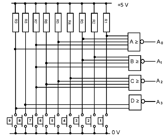
FIGURE 5.2: DECIMAL-TO-BINARY ENCODER
5.2.1 Switch 1 (4)
5.2.2 Switch 5 (4)
5.2.3 Briefly describe the STATE of the input switches if all outputs are ZERO. (2)
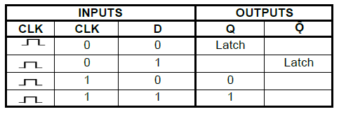
5.3 FIGURE 5.3 below represents the logic symbol of a clocked D-type flip-flop.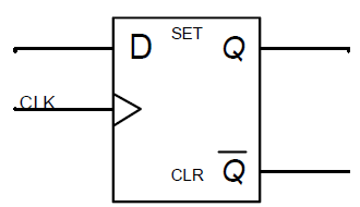
FIGURE 5.3
5.3.1 Draw the logic circuit of this flip-flop using NAND gates, NOR gates and an inverter. (6)
5.3.2 Complete the truth table of this flip-flop in TABLE 5.3.2 on ANSWER SHEET 5.3.2.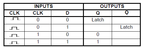 (4)
(4)
TABLE 5.3.2
5.4 State ONE application of the up/down counter. (1)
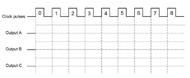
5.5 FIGURE 5.5 below shows a three-stage asynchronous ripple counter. Complete the timing diagram on ANSWER SHEET 5.5.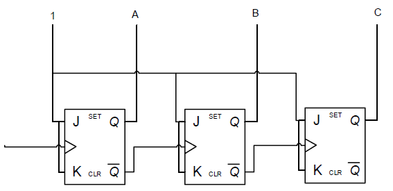 (8)
(8)
FIGURE 5.5: ASYNCHRONOUS RIPPLE COUNTER
5.6 Explain why the circuit in FIGURE 5.5 is called asynchronous. (3)
5.7 With reference to counters, explain the term propagation delay. (2)
5.8 Name TWO disadvantages of propagation delay. (2)
5.9 Explain the disadvantage of up/down counters in relation to normal up or down counter. (2)
5.10 Explain the difference between a full sequence counter and a truncated counter. (4)
5.11 Name TWO applications of counters. (2)
5.12 State how many clock pulses the following shift registers need to shift a 4-bit input from the input to the output. Each shift register consists of four D-type flip-flops.
5.12.1 Serial in-serial out shift register (SISU) (1)
5.12.2 Serial in-parallel out shift register (SIPO) (1)
5.12.3 Parallel in-parallel out shift register (PIPO) (1)
5.13 Explain how a parallel in-serial out shift register (PISO) consisting of four D-type flip-flops will shift a 4-bit input to the output. (4)
[55]
QUESTION 6: MICROCONTROLLERS
6.1 State TWO uses of a microcontroller in industrial control devices. (2)
6.2 State the basic function that the random access memory (RAM) performs. (2)
6.3 State the basic function of a read-only memory (ROM). (2)
6.4 Refer to communication in a microcontroller and answer the questions that follow.
6.4.1 Draw the block diagram of a microcontroller, clearly indicating the THREE system buses. (9)
6.4.2 Define the term interface. (2)
6.5 Refer to registers within the CPU and answer the questions that follow.
6.5.1 Explain the function of a programme counter. (3)
6.5.2 Explain the function of a memory address register. (2)
6.6 State ONE type of communication protocol. (1)
6.7 Define communication protocol. (2)
6.8 Illustrate the following data transfer methods with a block diagram:
6.8.1 Serial (4)
6.8.2 Parallel (4)
6.9 Refer to a serial communication interface and answer the questions that follow.
6.9.1 Write out the acronym UART in full. (1)
6.9.2 Explain the function of the UART. (4)
6.10 Refer to software of microcontrollers and answer the questions that follow.
6.10.1 Explain the term flowchart. (2)
6.10.2 Define an algorithm. (2)
6.10.3 Describe an instruction cycle. (3)
6.11 With reference to flowcharts, identify the following symbols:
6.11.1  (1)
(1)
6.11.2  (1)
(1)
6.12 Draw the symbol for a terminator in a flowchart. (1)
6.13 Explain where the symbol in QUESTION 6.11.1 is used in a flowchart. (2)
[50]
TOTAL: 200
FORMULA SHEET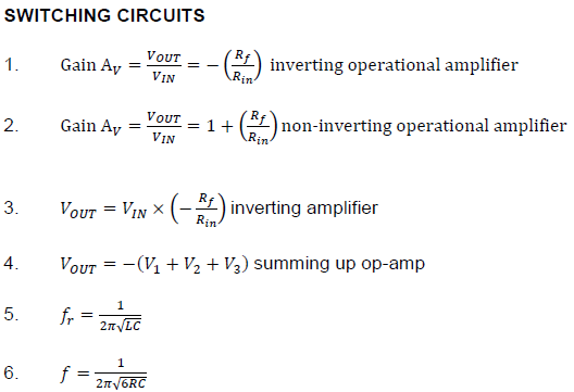
ANSWER SHEET 5.2.1 SEPTEMBER 2021
ANSWER SHEET 5.2.2 SEPTEMBER 2021
ANSWER SHEET 5.3.2 SEPTEMBER 2021
ANSWER SHEET 5.5