Electrical Technology: Electronics Grade 12 Questions - NSC Past Papers And Memos September 2020 Preparatory Examinations
Share via Whatsapp Join our WhatsApp Group Join our Telegram GroupINSTRUCTIONS AND INFORMATION
- This question paper consists of FIVE questions.
- Answer ALL the questions.
- Answer the following questions on the attached ANSWER SHEETS:
QUESTION 4.4.1
QUESTION 4.5.4
QUESTION 4.6.2 - Write your FULL NAME and CLASS SECTION on every ANSWER SHEET and hand them in with your ANSWER BOOK, whether you have used them or not.
- Sketches and diagrams must be large, neat and FULLY LABELLED.
- Show ALL calculations and round off answers correctly to TWO decimal places.
- Number the answers correctly according to the numbering system used in this question paper.
- You may use a non-programmable calculator.
- Calculations must include:
9.1 Formulae and manipulations where needed
9.2 Correct replacement of values
9.3 Correct answer and relevant units where applicable - A formula sheet is attached at the end of this question paper.
- Write neatly and legibly.
QUESTIONS
QUESTION 1: OCCUPATIONAL HEALTH AND SAFETY
1.1 Define the term accident, with reference to the Occupational Health and Safety Act, 1993 (Act 85 of 1993). (2)
1.2 Explain TWO general duties of employees in the workplace. (2)
1.3 Give TWO unsafe acts in a school workshop that can cause an accident. (2)
1.4 Briefly explain a third-degree burn. (2)
1.5 State TWO functions of a health and safety representative. (2)
[10]
QUESTION 2: RLC
2.1 Explain the phase relationship between current and voltage in the following AC circuit:
2.1.1 Pure capacitive circuit (2)
2.1.2 Pure inductive circuit (2)
2.1.3 Resistive circuit (2)
2.2 Refer to the circuit diagram FIGURE 2.2 below and answer the questions that follow.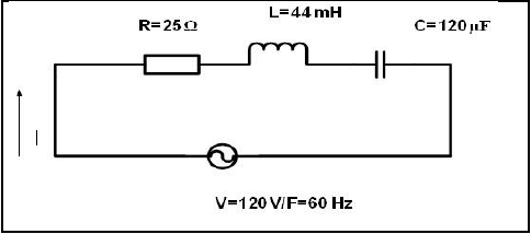
FIGURE 2.2: RLC CIRCUIT
Calculate:
2.2.1 Inductive reactance (3)
2.2.2 Capacitive reactance (3)
2.2.3 Impedance of the circuit (3)
2.2.4 Total current flow through the circuit (3)
2.3 Explain how the value of the capacitive reactance will be affected if the supply frequency is increased. (3)
2.4 A parallel circuit in FIGURE 2.4 consists of a capacitor that draws a current of 4 A, an inductor that draws a current of 6 A and a resistor that draws a current of 5 A. All the components are connected to a 240 V / 50 Hz supply.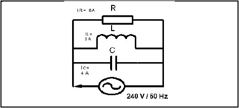
FIGURE 2.4: RLC PARALLEL CIRCUIT
Calculate:
2.4.1 Total current through the circuit (3)
2.4.2 The phase angle (3)
2.4.3 Inductive reactance (3)
2.4.4 Capacitive reactance (3)
2.5 A parallel RLC circuit consists of a 10 Ω resistor, a 0,05 µF and a 0,2 H inductor connected across a 120 V supply. Calculate the:
2.5.1 Resonant frequency (3)
2.5.2 Q-factor (4)
2.5.3 Bandwidth (3)
2.6 A series RLC tuned circuit has a resonant frequency of 95 MHz and a bandwidth of 200 kHz. The capacitor is 2,5 pF and the wire used to wind the coil has zero resistance. Calculate:
2.6.1 The Q factor of the circuit (3)
2.6.2 The size of the inductor (2)
2.6.3 The circuit resistance (2)
[50]
QUESTION 3: SEMICONDUCTORS
3.1 Explain the purpose of a field effect transistor. (2)
3.2 State the main advantage of field-effect devices over bipolar junction devices. (4)
3.3 Draw and label a symbol for the P-channel enhancement MOSFET. (3)
3.4 State TWO applications of an unijunctiontransistor (UJT). (2)
3.5 List THREE ideal properties of an ideal Op Amp. (3)
3.6 Describe the differences between the inverting and non-inverting inputs of an Op amp. (2)
3.7 Draw and label the symbol of a Darlington pair transistor. (4)
3.8 Explain the advantage of using negative feedback with an Op amp. (3)
3.9 Refer to FIGURE 3.9 and calculate the gain of the amplifier if the feedback resistor has a value of 120 kΩ and input resistor has a value of 12 kΩ.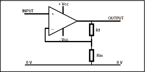
FIGURE 3.9: NON-INVERTING AMPLIFIER (3)
3.10 Refer to FIGURE 3.10 below and answer the questions that follow.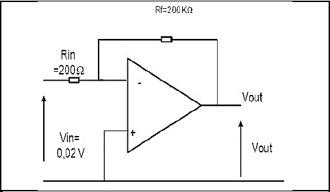
FIGURE 3.10: INVERTING OP-AMP
3.10.1 Calculate the gain of the Op amp. (3)
3.10.2 Calculate the output voltage. (3)
3.11 Explain the purpose of the comparator. (2)
3.12 List THREE modes of operation of a 555 timer IC. (3)
3.13 Explain the purpose of the THREE internally connected series resistor in a 555 IC. (3)
[40]
QUESTION 4: SWITCHING CIRCUITS
4.1 Explain the purpose of an astable multivibrator. (2)
4.2 Draw a fully labelled circuit diagram of a 741 astable multivibrator circuit. (5)
4.3 Refer to FIGURE 4.3 below and answer the questions that follow.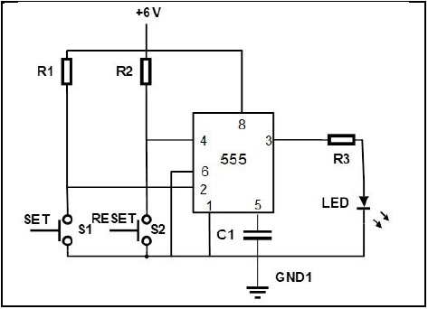
FIGURE 4.3: BISTABLE MULTIVIBRATOR
4.3.1 State the function of R1 and R2. (2)
4.3.2 Describe what happens when the set switch, S1 is pressed. (3)
4.3.3 Explain why threshold pin 6 is connected directly to ground. (3)
4.4 FIGURE 4.4 below shows input trigger pulses A and B to a 555 mono- stable multivibrator. Answer the questions that follow.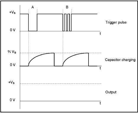
FIGURE 4.4: MONOSTABLE MULTIVIBRATOR TRIGGER PULSE
4.4.1 Draw the output signal on ANSWER SHEET 4.4.1. (4)
4.4.2 Describe the condition that occurred at trigger pulse B. (2)
4.4.3 Explain why the condition that occured at trigger pulse B does NOT affect the capacitor charging. (3)
4.5 Refer to FIGURE 4.5.1 below and answer the questions that follow.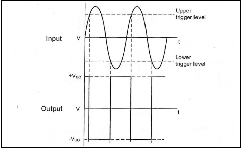
FIGURE 4.5.1: SCHMITT TRIGGER INPUT AND OUTPUT
4.5.1 State whether the output signal represents an inverting or non- inverting Schmitt trigger. Motivate your answer. (3)
4.5.2 Draw the circuit diagram of a Schmitt trigger consisting of TWO resistors and a 741 op-amp that will produce the output signal in FIGURE 4.5.1. (7)
4.5.3 Name TWO transducers that can be used as input devices to the Schmitt trigger. (2)
4.5.4 Draw the output signal on ANSWER SHEET 4.5.4 if the input signal in FIGURE 4.5.4 below is applied to the circuit.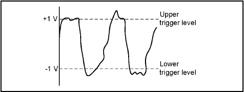
FIGURE 4.5.4: INPUT SIGNAL (4)
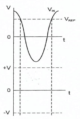
4.6 Refer to FIGURE 4.6 below and answer the questions that follow.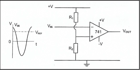
FIGURE 4.6: OP-AMP CIRCUIT DIAGRAM
4.6.1 Identify the op-amp circuit diagram in FIGURE 4.6. (2)
4.6.2 Draw the output signal on the ANSWER SHEET for QUESTION 4.6.2. (4)
4.6.3 Explain how the reference voltage is made negative. (2)
4.7 Refer to FIGURE 4.7 below and answer the questions that follow.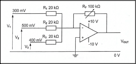
FIGURE 4.7: INVERTING SUMMING AMPLIFIER
Given:
- V1 = 300 mV
- V2 = 500 mV
- V3 = 400 mV
- RF = 100 kΩ
- R1 = R2 = R3 = 20 kΩ
4.7.1 Explain how the gain of this amplifier can be determined. (3)
4.7.2 Calculate the output voltage of the amplifier. (3)
4.7.3 Give a reason why the amplifier is NOT saturated. (2)
4.7.4 Calculate the gain of the amplifier using voltage values. (3)
4.7.5 Describe what will happen to the output voltage if the value of R2 is changed to 10 kΩ. (1)
[60]
QUESTION 5: AMPLIFIERS
5.1 Refer to FIGURE 5.1 below and answer the following questions.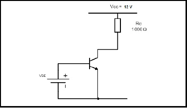
FIGURE 5.1
Calculate:
5.1.1 The voltage across the resistor (VCE) (2)
5.1.2 The maximum current (3)
5.2 Explain TWO advantages of class AB amplifiers. (2)
5.3 A 741 operational amplifier has an open loop gain of 100. It is connected into a negative feedback circuit which feeds back 9% of the output signal.
Answer the following questions.
5.3.1 Draw the circuit diagram of a negative feedback. (5)
5.3.2 Name THREE advantages of negative feedback (3)
5.3.3 Calculate the overall gain of negative feedback. (3)
5.4 State TWO advantages of a transformer coupled amplifier. (2)
5.5 List TWO uses for RF amplifiers. (2)
5.6 State TWO advantages of a push pull amplifier. (2)
5.7 Refer to an RC-phase shift oscillator and answer the following questions.
5.7.1 Write down the formula to calculate the resonant frequency of a phase shift oscillator. (2)
5.7.2 Draw a circuit diagram of a RC phase shift oscillator. (6)
5.7.3 State TWO advantages of the RC network. (2)
5.7.4 Explain the type of feedback used by the RC phase shift oscillator. (3)
5.7.5 List THREE important areas on a frequency response curve. (3)
[40]
TOTAL: 200
FORMULA SHEET: ELECTRICAL TECHNOLOGY
ANSWER SHEETS
ANSWER SHEET 4.4.1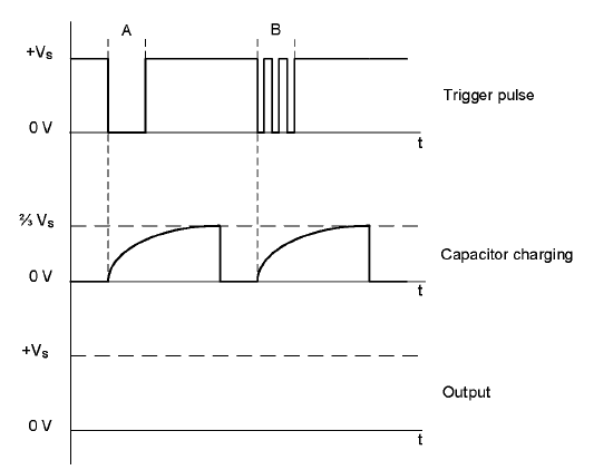
ANSWER SHEET 4.5.4 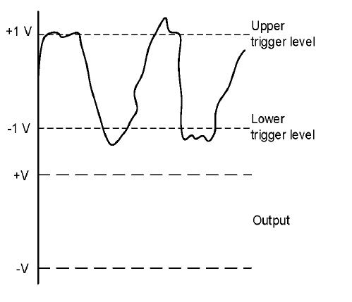
ANSWER SHEET 4.6.2