Electrical Technology: Digital Grade 12 Questions - NSC Past Papers And Memos September 2020 Preparatory Examinations
Share via Whatsapp Join our WhatsApp Group Join our Telegram GroupINSTRUCTIONS AND INFORMATION
- This question paper consists of FIVE questions.
- Answer ALL the questions.
- Answer the following questions on the attached ANSWER SHEETS:
QUESTIONS 2.4.1, 2.5.4, 2.6.2 and 3.1.3
QUESTIONS 4.3, 4.4.3, 4.5.2 and 4.6.2 - Write your FULL NAME and CLASS on every ANSWER SHEET and hand them in with your ANSWER BOOK, whether you have used them or not.
- Sketches and diagrams must be large, neat and FULLY LABELLED.
- Show ALL calculations and round off answers correctly to TWO decimal places.
- Number the answers correctly according to the numbering system used in this question paper.
- You may use a non-programmable calculator.
- Calculations must include:
9.1 Formulae and manipulations where needed
9.2 Correct replacement of values
9.3 Correct answer and relevant units where applicable - A formula sheet is attached at the end of this question paper.
- Write neatly and legibly.
QUESTIONS
QUESTION 1: OCCUPATIONAL HEALTH AND SAFETY
1.1 Define the term accident with reference to the Occupational Health and Safety Act, 1993 (Act 85 of 1993). (2)
1.2 Explain TWO general duties of employees in the workplace. (2)
1.3 State TWO unsafe conditions in a school workshop that can cause an accident. (2)
1.4 Briefly explain a third-degree burn. (2)
1.5 State TWO functions of a health and safety representative. (2)
[10]
QUESTION 2: SWITCHING CIRCUITS
2.1 Explain the purpose of an astable multivibrator. (2)
2.2 Draw a fully labelled circuit diagram of a 741 astable multivibrator circuit. (5)
2.3 Refer to FIGURE 2.3 below and answer the questions that follow.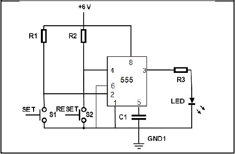
FIGURE 2.3: BISTABLE MULTIVIBRATOR
2.3.1 State the function of R1 and R2. (2)
2.3.2 Describe what happens when the set switch, S1 is pressed. (3)
2.3.3 Explain why threshold pin 6 is connected directly to ground. (3)
2.4 FIGURE 2.4 below shows input trigger pulses A and B to a 555 monostable multivibrator. Answer the questions that follow.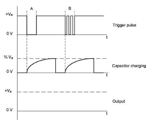
FIGURE 2.4: MONOSTABLE MULTIVIBRATOR TRIGGER PULSES
2.4.1 Draw the output signal on ANSWER SHEET 2.4.1. (4)
2.4.2 Describe the condition that occurred at trigger pulse B. (2)
2.4.3 Explain why the condition that occurs at trigger pulse B does NOT affect the capacitor charging. (3)
2.5 Refer to FIGURE 2.5 below and answer the questions that follow.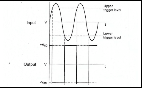
FIGURE 2.5: SCHMITT TRIGGER INPUT AND OUTPUT
2.5.1 State whether the output signal represents an inverting or non- inverting Schmitt trigger. Motivate your answer. (3)
2.5.2 Draw the circuit diagram of a Schmitt trigger consisting of TWO resistors and a 741 op-amp that will produce the output signal in FIGURE 2.5. (7)
2.5.3 Name TWO transducers that can be used as input devices to the Schmitt trigger. (2)
2.5.4 Draw the output signal on ANSWER SHEET 2.5.4 if the input signal in FIGURE 2.5.4 below is applied to the circuit.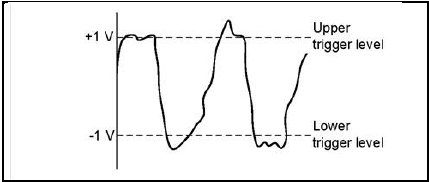
FIGURE 2.5.4: INPUT SIGNAL (4)
2.6 Refer to FIGURE 2.6 below and answer the questions to follow.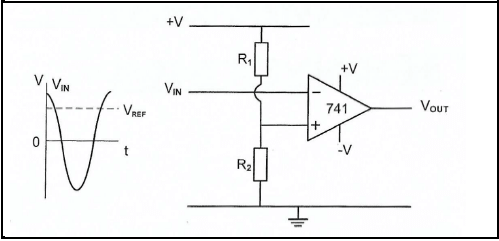
FIGURE 2.6: OP-AMP CIRCUIT DIAGRAM
2.6.1 Identify the op-amp circuit diagram in FIGURE 2.6. (2)
2.6.2 Draw the output signal on the ANSWER SHEET for QUESTION 2.6.2. (4)
2.6.3 Explain how the reference voltage is made negative. (2)
2.7 Refer to FIGURE 2.7 below and answer the questions that follow.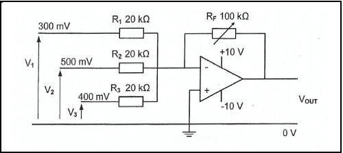
FIGURE 2.7: INVERTING SUMMING AMPLIFIER
Given:
- V1 = 300 mV
V2 = 500 mV
V3 = 400 mV
RF = 100 kΩ
R1 = R2 = R3 = 20 kΩ
2.7.1 Explain how the gain of this amplifier can be determined. (3)
2.7.2 Calculate the output voltage of the amplifier. (3)
2.7.3 Give a reason why the amplifier is NOT saturated. (2)
2.7.4 Calculate the gain of the amplifier using voltage values. (3)
2.7.5 Describe what will happen to the output voltage if the value of R2 is changed to 10 kΩ. (1)
[60]
QUESTION 3: SEMICONDUCTOR DEVICES
3.1 Refer to FIGURE 3.1 below and answer the questions that follow.
FIGURE 3.1: 741 OP-AMP
3.1.1 State how you would identify pin 1 of the Integrated Circuit (IC) in FIGURE 3.1. (1)
3.1.2 Give TWO reasons why negative feedback is important when the amplifier is used as a linear amplifier. (2)
3.2 FIGURE 3.2 below shows the op-amp as an inverting amplifier. Calculate the output voltage based on the data given in the circuit.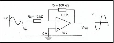
FIGURE 3.2 INVERTING OP-AMP
Given:
- VIN = 2 V
- RF = 100 kΩ
- RIN = 12 kΩ (3)
3.3 Rewrite the abbreviation DIP in full. (1)
3.4 Name THREE modes of operation of the NE555 IC. (3)
3.5 Explain what will happen to the output of a NE555 IC when the trigger voltage rises above the threshold voltage level of 10 V. (2)
3.6 Explain the function of threshold Pin 6 with regards to a 555 timer IC. (3)
3.7 Define the term flip flop. (2)
3.8 Define the term monolithic. (2)
3.9 Explain the term open loop gain. (2)
3.10 State the operating voltages of an Op-Amp. (2)
3.11 The internal circuit of an Op-Amp is grouped into three stages.
- A differential amplifier
- High gain differential amplifier
- Common collector circuit
With reference to the above information answer the questions that follow.
3.11.1 Explain the function of the high gain differential stage. (2)
3.11.2 Name TWO characteristics of the common collector stage. (2)
3.11.3 Explain the principle of operation of the common collector stage. (3)
3.12 FIGURE 3.12 below shows a 741 op-amp. Answer the questions that follow.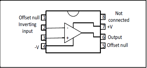
FIGURE 3.12: 741 OP-AMP
3.12.1 Label pin 3. (1)
3.12.2 Name the type of package in which the integrated circuit (IC) above is constructed. (1)
3.13 Draw the output signal on ANSWER SHEET 3.13 if the signals in FIGURE 3.13 below are applied to the inputs of an op-amp.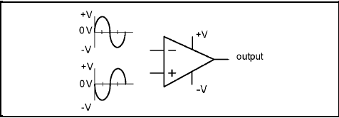 (2)
(2)
FIGURE 3.13: SIGNALS
3.14 Explain the operation of the 555 timer when connected in monostable mode. (4)
3.15 Name the TWO primary building blocks a 555 timer consists of. (2)
[40]
QUESTION 4: DIGITAL AND SEQUENTIAL DEVICES
4.1 Briefly explain how a liquid crystal display (LCD) controls the passing of light through it. (3)
4.2 Refer to an LED seven-segment display and illustrate the difference between a sinking output and a sourcing output by using TWO simple circuit diagrams. (4)
4.3 Study FIGURE 4.3 below of a decimal-to-binary encoder. Use the table on ANSWER SHEET 4.3 to complete the truth table.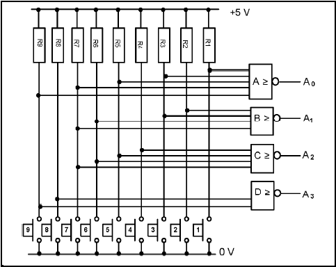
FIGURE 4.3: DECIMAL-TO-BINARY ENCODER (10)
4.4 FIGURE 4.4 below is the block diagram of a BCD-to-seven-segment decoder connected to a seven-segment LED display. Answer the questions that follow.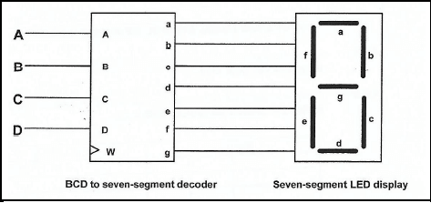
FIGURE 4.4: BCD TO SEVEN SEGMENT DECODER CONNECTED TO SEVEN SEGMENT LED DISPLAY
4.4.1 Label input W. (1)
4.4.2 Explain the function of the driver transistors found in the BCD to seven-segment display decoder. (3)
4.4.3 Complete the truth table of a BCD to seven-segment decoder connected to a seven-segment LED display in TABLE 4.4.3 on the ANSWER SHEET for QUESTION 4.4.3.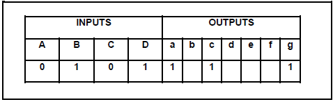
TABLE 4.4.3: BCD TRUTH TABLE (4)
4.5 FIGURE 4.5 below represents the logic symbol of a HALF ADDER. Answer the questions that follow.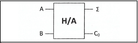
FIGURE 4.5: LOGIC SYMBOL OF A HALF ADDER
4.5.1 Draw the logic circuit of this half adder using an AND gate and an EXLUSIVE OR gate only. (4)
4.5.2 Complete the truth table of the half adder in TABLE 4.5.2 on the ANSWER SHEET for QUESTION 4.5.2.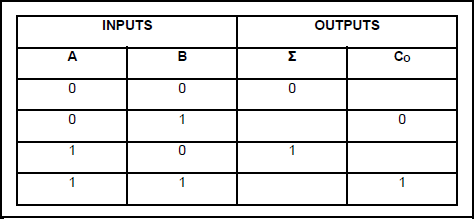
TABLE 4.5.2: TRUTH TABLE FOR HALF ADDER (4)
4.6 FIGURE 4.6 below represents the logic symbol of a J-K flip-flop. Answer the questions that follow.
FIGURE 4.6: LOGIC SYMBOL OF J-K FLIP-FLOP
4.6.1 Draw the logic circuit of this flip-flop using AND gates and NOR gates. (7)
4.6.2 Complete the truth table of the flip-flop below on ANSWER SHEET 4.6.2.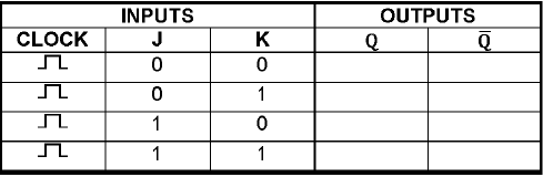
TABLE 4.6.2: TRUTH TABLE (4)
4.7 Explain the difference between a synchronous counter and an asynchronous counter. (2)
4.8 Draw a fully labelled circuit diagram of a four-stage Asynchronous Binary-to-BCD counter using four JK flip-flops and a NAND gate. (9)
[55]
QUESTION 5: MICROCONTROLLERS
5.1 State TWO uses of microcontrollers. (2)
5.2 State TWO advantages of a microcontroller. (2)
5.3 With reference to the hardware of microcontrollers, answer the questions that follow.
5.3.1 Explain the function of the current instruction register (CIR). (2)
5.3.2 State the purpose of an analogue-to-digital converter (ADC). (2)
5.4 With reference to the Central Processing Unit (CPU) of a microcontroller, answer the questions that follow.
5.4.1 Briefly define a register. (2)
5.4.2 Describe the function of a register. (2)
5.4.3 Name TWO types of registers that are used in the CPU of a microcontroller. (2)
5.4.4 Explain the function of the memory data register. (2)
5.5 Draw a fully labelled circuit diagram of a simple counter/timer. (6)
5.6 Define the following elements in a microcontroller:
5.6.1 Protocol (1)
5.6.2 Hardware interface (2)
5.7 Discuss the read-only memory (ROM) with reference to the CPU of a microcontroller. (3)
5.8 With reference to communication in a microcontroller, answer the questions to follow.
5.8.1 Name TWO methods of sending data. (2)
5.8.2 State the advantages of parallel communication. (2)
5.8.3 Name the disadvantages of synchronous communication. (3)
[35]
TOTAL: 200
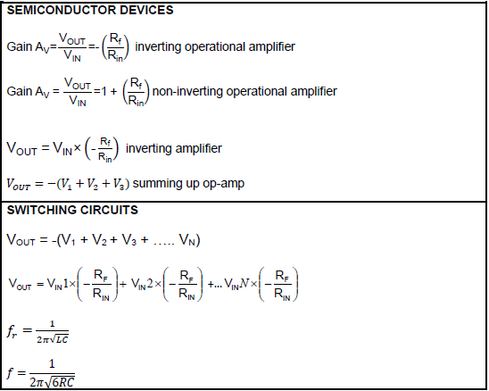
FORMULA SHEET
ANSWER SHEETS
ANSWER SHEET 2.4.1
ANSWER SHEET 2.5.4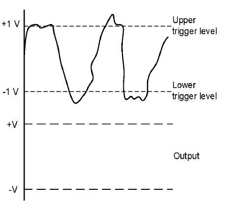
ANSWER SHEET 2.6.2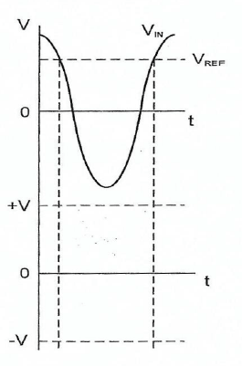
ANSWER SHEET 3.13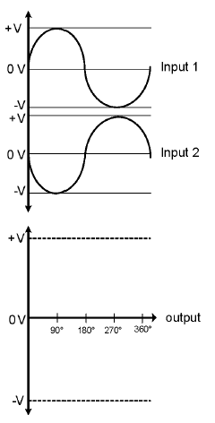
ANSWER SHEET 4.3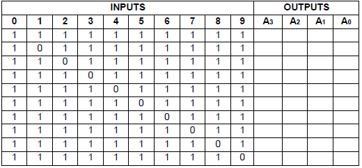
ANSWER SHEET 4.4.3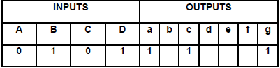
ANSWER SHEET 4.5.2
ANSWER SHEET 4.6.2