Electrical Technology: Electronics Grade 12 Memorandum - NSC Exams Past Papers and Memos September 2019 Preparatory Examinations
Share via Whatsapp Join our WhatsApp Group Join our Telegram GroupINSTRUCTIONS TO MARKERS
- All questions with multiple answers imply that any relevant, acceptable answer should be considered.
2. Calculations:
2.1 All calculations must show the formulae.
2.2 Substitution of values must be done correctly.
2.3 All answers MUST contain the correct unit to be considered.
2.4 Alternative methods must be considered, provided that the correct answer is obtained.
2.5 Where an incorrect answer could be carried over to the next step, the first answer will be deemed incorrect. However, should the incorrect answer be carried over correctly, the marker has to re-calculate the values, using the incorrect answer from the first calculation. If correctly used, the candidate should receive the full marks for subsequent calculations.
2.6 Markers should consider that candidates' answers may deviate slightly from the marking guideline depending on how and where in the calculation rounding off was used. - These marking guidelines are only a guide with model answers.
- Alternative interpretations must be considered and marked on merit. However, this principle should be applied consistently throughout the marking session at ALL marking centres.
MEMORANDUM
QUESTION 1: OCCUPATIONAL HEALTH AND SAFETY (GENERIC)
1.1
- Faulty tools or equipment ✓
- Poor ventilation ✓
- Poor quality of or missing guards on machines ✓
- Excessive noise
- Lack of knowledge of emergency procedures
(Any THREE relevant answers) (3)
1.2 The purpose of the Occupational Health and Safety Act is to provide for the health and safety of:
- Persons at work ✓
- Persons in connection with the use of plant and machinery ✓
- The protection of persons against hazards arising out of the activities of other persons at work
- To establish an advisory council for occupational health and safety and related matters (2)
1.3
- Horseplay ✓
- Running in the workshop ✓
- Throwing things around
- Leaving bags, stools/chairs or material in walkway
- Spilling a liquid or oil without cleaning
- (Any relevant answer) (2)
1.4
- Keep person lying down ✓
- Cover the person to maintain body heat ✓
- Do not move the person in case of neck or spine injuries ✓
- If unconscious, put them on their side (recovery position)
(Any THREE relevant answers) (3) [10]
QUESTION 2: RLC CIRCUITS (GENERIC)
2.1 Q-factor for a parallel circuit concerns the relationship between the resistance and the reactance of the circuit ✓
The Q-factor of the circuit is found from the ratio between the reactive components either the inductive or capacitance at resonance and the active power of the resistance ✓ (2)
2.2 Factors that affect the impedance of an RLC circuit:
- Frequency ✓
- Inductance ✓
- Capacitance ✓ (3)
2.3
- Z = R ✓
- XL = XC ✓
- Cos θ = 1 ✓
- R = minimum
- I = maximum (Any THREE) (3)
2.4
2.4.1 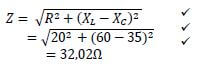 (3)
(3)
2.4.2 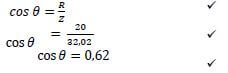 (3)
(3)
2.4.3 lagging ✓ (1)
2.4.4 The Q-factor will be halved ✓because the Q-factor is inversely proportional to the resistance of the circuit. ✓ The doubling of the inductance and capacitance as a ratio will have no effect on the Q factor ✓ (3)
2.5
2.5.1 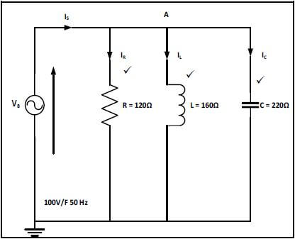 (3)
(3)
2.5.2
- I = V
R
=100
120
= 0,83A
2.5.3
- IL = V
XL
=100
160
= 0,625A
2.5.4
- IC = V
XC
=100
220
= 0,455A
2.5.5 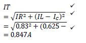
2.5.6
- cos θ =IR=
IZ
= cos-1 0,83
0,847
= 11,5° (3)
2.5.7 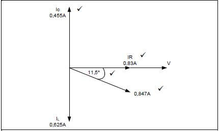 (4)
(4)
[40]
QUESTION 3: SEMICONDUCTOR DEVICES (SPECIFIC)
3.1 Junction field effect transistor (JFET) ✓and Metal oxide semiconductor (MOSFET) ✓ (2)
3.2
- The main advantage of a FET over A BJT is that it has significantly lower levels of power loss making it more efficient ✓
- FET’s also have high input resistance thus drawing very little current from the previous stage ✓ (2)
3.3
- A signal applied to the non-inverting terminal ✓will appear at the output terminal in the same direction as when it entered the op-amp ✓
- A signal applied to the inverting terminal will appear ✓ at the output terminal in an inverted direction as when it entered the op-amp ✓ (4)
3.4
- The mode of operation of a UJT is controlled by varying the value of Re which will change the amount of available current ✓
- A lower amount of current will not allow the UJT to saturate but rather force it to reset and re-trigger ✓ (2)
3.5
- Input stage (Differential amplifier) ✓
- Intermediate stage (High gain differential amplifier) ✓
- Common Collector (Darlington Pair) output stage ✓ (3)
3.6 The ability of the Op-amp to suppress a common-anode is called the common-mode rejection ratio ✓ (2)
3.7
3.7.1 Non-inverting Op-amp ✓ (1)
3.7.2
- AV = 1 + Rf
Rin
= 1 + 1000
1900 ✓
= 1 + 0,526
= 1,526 ✓ (2)
3.8
- Basic timing function, e.g. turning a light on or off after a period of time ✓
- Pulse oscillation and wave generation ✓
- Creating a flashing warning light ✓
- Digital logic probes
- Producing musical notes of specific frequencies
- Temperature measurement
- Controlling the positioning of servo devices (3)
3.9
- Only operate on supply voltages between +5V to + 18V ✓
- The maximum current it can either sink or source is 200 mA ✓ (2)
3.10
- In the construction of this IC there are three series connected resistors of identical value, 5 kΩ ✓
- These resistors divide the voltages to 2/3 ✓ and 1/3 ✓ of the supply voltage (3)
3.11 Threshold ✓ (1)
3.12
- This pin sets off the IC
- It is an active low trigger ✓
- When the voltage on pin 2 is less than 13of the supply, the output goes high ✓
- When the voltage on pin 2 is higher than 23of the supply, the output will go low ✓
- If connected to ground the output will go ‘high’ and remain ‘high’ (3) [30]
QUESTION 4: SWITCHING CIRCUITS (SPECIFIC)
4.1
4.1.1 Mono-stable multivibrator ✓ (1)
4.1.2
- It has ONE input ✓
- It has ONE stable state ✓ (2)
4.1.3
- The RC network in this circuit is the timing component of this circuit ✓
- The values of the resistor and the capacitor determine for how long the circuit will be in the HIGH ✓state before it reverts back to its stable LOW state ✓ (3)
4.1.4
- By changing R2 from a fixed resistor value to a variable resistor ✓
- By changing the value of C2 from a fixed value capacitor to a variable capacitor ✓
- By changing both R2 and C2 from fixed values ✓ to variable values ✓ (4)
4.1.5
- When the circuit is in resting condition, the negative voltage of -Vref on the inverting input serves to hold this inverting input low ✓
- This will cause the Op-Amp to saturate and the output to rise to and stay at +15 V ✓
- The capacitor, C, charges up with the top plate to + 15 V, and the bottom plate to 0 V ✓
- When the capacitor is charged, no current flows through R as there is no voltage over it. This holds the non-inverting input at 0 V ✓
- A positive trigger pulse larger than Vref applied to the inverting input terminal will raise the inverting input potential above the 0 V of the non-inverting input ✓
- The Op-Amp will now saturate and the output will go to -15 V ✓
- The capacitor will now immediately start discharging through the resistor Rf✓
- The lower plate of the capacitor rises to 0 V and when the voltage is less negative than Vref, the output changes to +15 V again ✓ (8)
4.1.6 Debouncing ✓ (1)
4.2 4.2.1 At one end the potentiometer will be connected to 0 Ω. ✓ R1 will prevent the full supply flowing to pin 6 and 7, when the potentiometer is in the 0 Ω position ✓ (2)
4.2.2
- By changing the value of C1 ✓
- By changing the value of R3 ✓ (2)
4.2.3 The time period will increase ✓ (1)
4.3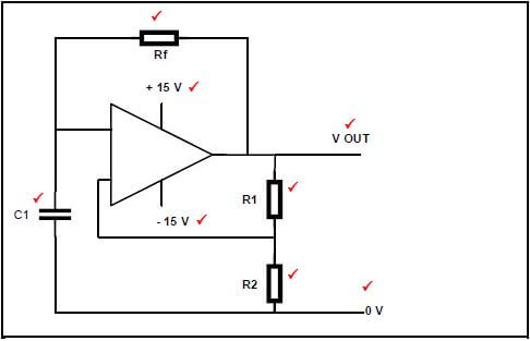 (8)
(8)
4.4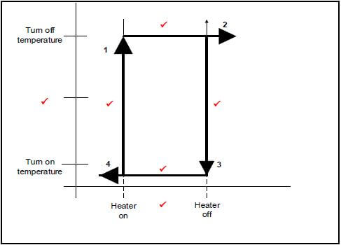 (6)
(6)
4.5 The time lag (delay) between cause ✓ and effect ✓ (2)
4.6
- First stage of many radio receivers to clean up noise ✓
- To eliminate switch bounce in digital circuits ✓
- Varying input waveforms, for instance sine wave changed into square wave or rectangular wave
- Signal recovery after experiencing severe distortion (2)
4.7 (8)
(8)
4.8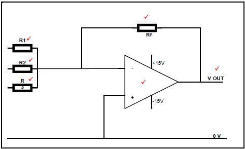 (6)
(6)
4.9 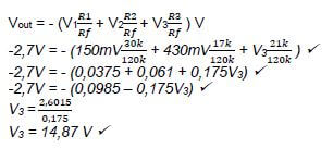
(4) [60]
QUESTION 5: AMPLIFIERS (SPECIFIC)
5.1 Class B amplification is when the output collector current of the amplifier ✓ only flows for the input cycle ✓ (2)
5.2
5.2.1
- VCC =VCE + ICRC ✓
VCC = VCE ✓✓when the transistor is OFF and collector current is not flowing
VCE = 9 v ✓ (4)
5.2.2
- IC = VC
RC
=9
750√
= 12 mA√ (3)
5.2.3
(3)
5.3
- RF communications ✓
- Optical fibre communications ✓
- Pre-amplifiers in public address systems ✓
- Small signal amplifiers in radio or TV receivers (3)
5.4
- Improving the amplifier’s stability ✓
- Increasing the amplifier’s bandwidth ✓
- Enhancing the amplifier’s input and output impedances ✓
- Reducing or suppressing a noise produced with the amplifier (3)
5.5
- Low frequency area ✓
- Middle frequency area ✓
- High frequency area (2)
5.6
5.6.1
- AV = 20Log10EOUT√
EIN
AV = 20Log106.2√
4
AV = 20 × 1.55
AV = 31 dB √ (3)
5.6.2
- Ap = 10 log10Pout
Pin√
Ap = 10log10 29
850×10−3 √
Ap = 341.2dB √ (3)
5.7
- Class AB ✓
- Class AB does not allow a transistor to move into its cut-off region, ✓ so it eliminates the distortion ✓ (3)
5.8 Radio frequency amplifiers are designed to amplify ✓ a single high frequency ✓ (2)
5.9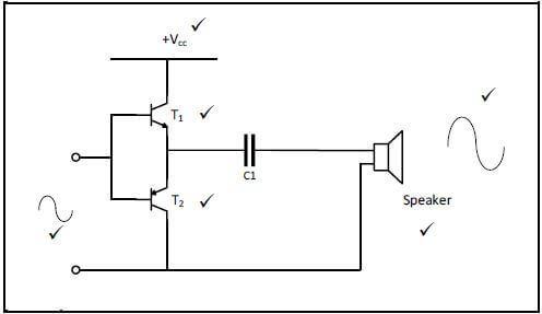 (6)
(6)
5.10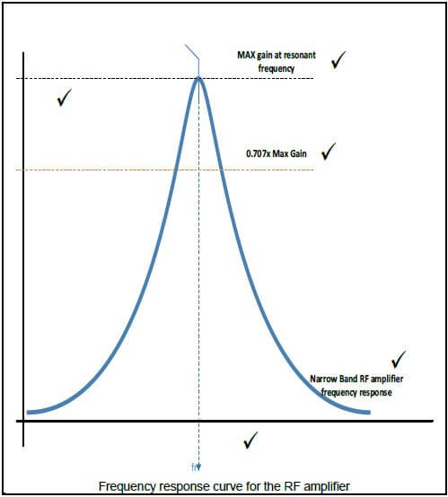 (6)
(6)
5.11
5.11.1 Positive feedback ✓ (1)
5.11.2 RC phase shift oscillator is widely used in the lower audio frequency AF range up to 10 kHz ✓ (1)
5.12
5.12.1 RF coil offers resistance against the change in the collector current ✓ and causes the collector voltage Vc to decrease ✓ (2)
5.12.2 The tank circuit receives energy from a DC source ✓and converts that energy into a sinusoidal signal at a frequency determined by the inductor and capacitor ✓ (2)
5.12.3
- Hartley oscillator tank circuit consists of two inductors and one capacitor ✓
- Colpitts oscillator tank circuit consists of two capacitors and one inductor ✓ (2)
5.13
- Poor frequency response. Gain is constant over only a small range of frequencies ✓
- Increased cost ✓
- Tends to introduce hum in the output ✓
- Low frequency receives less amplification than high frequencies ✓ (4)
5.14
- They isolate each stage by blocking the DC voltage of one stage ✓ from affecting the next. ✓ They allow AC signals to pass freely from one stage to the next ✓ (3)
5.15
- Resistance capacitance coupling ✓
- Transformer coupling ✓ (2) [60]
TOTAL: 200