Electrical Technology: Electronics Grade 12 Questions - NSC Exams Past Papers and Memos September 2019 Preparatory Examinations
Share via Whatsapp Join our WhatsApp Group Join our Telegram GroupINSTRUCTIONS AND INFORMATION
- This question paper consists of FIVE questions.
- Sketches and diagrams must be large, neat and fully labelled.
- Show ALL calculations and round off answers to TWO decimal places. Show the units for ALL answers of calculations.
- Number the answers correctly according to the numbering system used in this question paper.
- You may use a non-programmable calculator.
- A formula sheet is provided at the end of this question paper.
- Write neatly and legibly.
QUESTIONS
QUESTION 1: OCCUPATIONAL HEALTH AND SAFETY (GENERIC)
1.1 Name THREE unsafe conditions that cause most accidents in the workshop. (3)
1.2 Explain the purpose of the Occupational Health and Safety Act. (2)
1.3 Give TWO unsafe acts in a school workshop that can cause an accident. (2)
1.4 Describe THREE standard treatments for electric shock after the electricity has been removed. (3) [10]
QUESTION 2: RLC CIRCUITS (GENERIC)
2.1 Define the term Q-factor with reference to a parallel resonant circuit. (2)
2.2 State THREE factors that will affect the impedance of an RLC circuit. (3)
2.3 List THREE characteristics of a series resonance frequency. (3)
2.4 Refer to FIGURE 2.4 below and answer the questions that follow.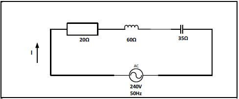
FIGURE 2.4: RLC CIRCUIT
Given:
R = 20 Ω
XL = 60 Ω
XC = 35 Ω
VS = 240 V
F = 50 Hz
2.4.1 Calculate the total impedance of the circuit. (3)
2.4.2 Calculate the power factor of the circuit. (3)
2.4.3 State whether the power factor is leading or lagging (1)
2.4.4 Explain what happens to the Q-factor of an RLC circuit if the values of R, L and C are doubled. (3)
2.5 A parallel RLC circuit consists of a resistor with a resistance of 120 Ω, an inductor with an inductive reactance of 160 Ω and a capacitor with a capacitive reactance of 220 Ω. All are connected across a 100 V/50 Hz supply.
2.5.1 Draw the circuit diagram that represents the above information. (3) Calculate:
2.5.2 The current through the resistor (3)
2.5.3 The current through the inductor (3)
2.5.4 The current through the capacitor (3)
2.5.5 The total current of the circuit (3)
2.5.6 The phase angle (3)
2.5.7 Draw the phasor diagram that represents the current and the voltage. (4) [40]
QUESTION 3: SEMI-CONDUCTOR DEVICES (SPECIFIC)
3.1 List TWO types of field effect transistors. (2)
3.2 State the main advantage of a field effect transistor over a bipolar-junction transistor. (2)
3.3 Describe the difference between the inverting and the non-inverting amplifier of an Op-Amplifier. (4)
3.4 Explain how it is possible to control the mode of operation of a UJT. (2)
3.5 State the THREE stages of a 741 Op-Amp. (3)
3.6 Explain the term Common Mode Rejection Ratio. (2)
3.7 Refer to FIGURE 3.7 below and answer the questions that follow. 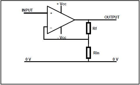
FIGURE 3.7: OP-AMPLIFIER
3.7.1 Identify the Op-Amplifier in FIGURE 3.7 (1)
3.7.2 Calculate the gain of the amplifier if the feedback resistor has a value of 1 kΩ and the input resistor has a value of 1 900 Ω. (2)
3.8 Name THREE uses for the 555 timer IC. (3)
3.9 Name TWO operating boundaries of a 555 timer IC. (2)
3.10 Explain the purpose of the three internally connected series resistors in a 555 IC. (3)
3.11 Refer to FIGURE 3.11 below. Label pin 6. (1)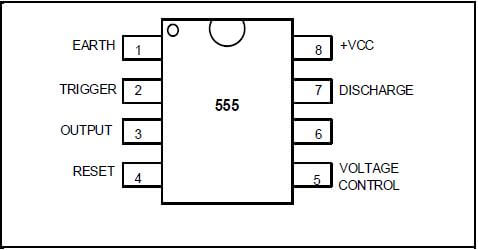
FIGURE 3.11: 555 TIMER
3.12 With reference to a 555 timer IC, explain the function of pin 2 (trigger). (3) [30]
QUESTION 4: SWITCHING CIRCUITS (SPECIFIC)
4.1 Refer to FIGURE 4.1 below and answer the questions that follow.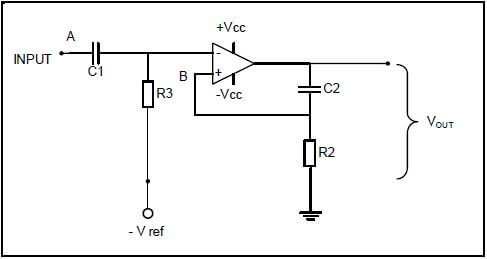
FIGURE 4.1: MULTIVIBRATOR
4.1.1 Identify the multivibrator in FIGURE 4.1. (1)
4.1.2 Name TWO characteristics of this multivibrator. (2)
4.1.3 Explain the function of the network C2 and R2. (3)
4.1.4 Analyse FIGURE 4.1 above and explain the THREE ways to change this circuit in order to have a variable time in the high state. (4)
4.1.5 Explain the principle of operation of the circuit in FIGURE 4.1. (8)
4.1.6 With reference to FIGURE 4.1, name ONE application of this multivibrator. (1)
4.2 Refer to FIGURE 4.2 above and answer the questions that follow. 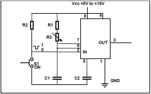
FIGURE 4.2: MULTIVIBRATOR
4.2.1 Explain the function of R1 in the circuit. (2)
4.2.2 Name TWO methods to vary the time period of this circuit. (2)
4.2.3 Explain the effect on the output waveform if R3 is changed from 10 kΩ to 27 kΩ. (1)
4.3 Draw a fully labelled circuit diagram of an Op-Amp Astable multivibrator circuit. (8)
4.4 With reference to the Schmitt trigger, draw a fully labelled hysteresis characteristic curve (6)
4.5 Define the term hysteresis with reference to the Schmitt trigger. (2)
4.6 Name TWO applications of the Schmitt trigger. (2)
4.7 Draw a fully labelled circuit diagram of a temperature sensor circuit. (8)
4.8 Draw a fully labelled circuit diagram of a summing amplifier with THREE inputs. (6)
4.9 A summing amplifier has three input resistors with the following values:
R1 = 30 kΩ, R2 = 17 kΩ, R3 = 21 kΩ
The output voltage for this circuit is given as -2,7 V.
The known input voltages are V1 = 150 mV, V2 = 430 mV.
Calculate the value of V3 if this circuit has a 120 kΩ feedback resistor. (4) [60]
QUESTION 5: AMPLIFIERS (SPECIFIC)
5.1 Explain Class B amplification with reference to the output collector. (2)
5.2 Refer to FIGURE 5.2 below and answer the questions that follow.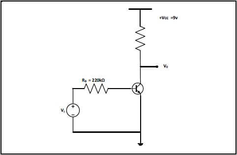
FIGURE 5.2: CLASS A FIXED BIASED TRANSISTOR AMPLIFER
5.2.1 Calculate the maximum collector voltage. (4)
5.2.2 Calculate the maximum collector current. (3)
5.2.3 Draw the circuit load line of the circuit. (3)
5.3 State THREE applications of an RC coupled amplifier. (3)
5.4 List THREE advantages of negative feedback. (3)
5.5 Describe TWO important areas on the frequency curve. (2)
5.6 Use the given information to answer the following questions:
5.6.1 Calculate the voltage gain, if the voltage measured across the input terminals of an amplifier is 4 V and 6,2 V at the output terminals. (3)
5.6.2 An 850 mW signal is introduced to the input of an amplifier. On emerging the signal has been amplified to 29 W. Calculate the amplifier gain. (3)
5.7 Name the circuit used to eliminate the effects of cross-over distortion and explain how it is able to do this. (3)
5.8 Explain the purpose of a Radio frequency amplifier. (2)
5.9 Draw a fully labelled circuit diagram of a push-pull amplifier. (6)
5.10 Draw a fully labelled frequency response curve for the RF amplifier. (6)
5.11 Refer to FIGURE 5.11 below and answer the questions that follow.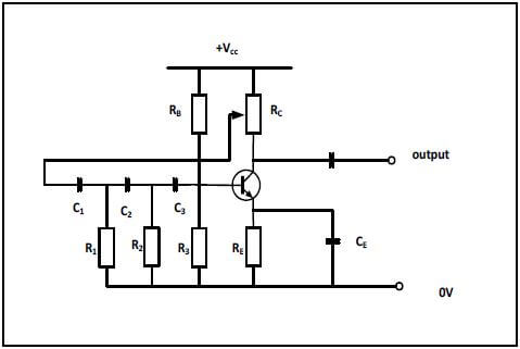
FIGURE 5.11: RC PHASE SHIFT OSCILLATOR
5.11.1 Name the type of feedback used in the above circuit diagram. (1)
5.11.2 State ONE application of the RC phase shift oscillator. (1)
5.12 FIGURE 5.12 refers to the Hartley oscillator. Answer the following questions. RF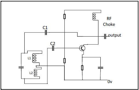
FIGURE 5.12: HARTLEY OSCILLATOR
5.12.1 Describe the function of the RF coil in the Hartley oscillator circuit. (2)
5.12.2 Discuss the purpose of the tank circuit in Hartley oscillators. (2)
5.12.3 Describe the difference between the Hartley oscillator and the Colpitts oscillator with reference to their tanks. (2)
5.13 List FOUR disadvantages of transformer coupling in amplifiers. (4)
5.14 Explain why DC blocking capacitors are used at the input and output of an amplifier. (3)
5.15 State TWO methods of inter-stage coupling. (2) [60]
TOTAL: 200