ELECTRICAL TECHNOLOGY (DIGITAL) GRADE 12 MEMORANDUM - NSC EXAMS PAST PAPERS AND MEMOS MAY/JUNE 2021
Share via Whatsapp Join our WhatsApp Group Join our Telegram GroupELECTRICAL TECHNOLOGY (DIGITAL)
GRADE 12
NATIONAL SENIOR CERTIFICATE EXAMINATIONS
MAY/JUNE 2021
INSTRUCTIONS TO THE MARKERS
- All questions with multiple answers imply that any relevant, acceptable answer should be considered.
- Calculations:
2.1 All calculations must show the formulae.
2.2 Substitution of values must be done correctly.
2.3 All answers MUST contain the correct unit to be considered.
2.4 Alternative methods must be considered, provided that the correct answer is obtained.
2.5 Where an incorrect answer could be carried over to the next step, the first answer will be deemed incorrect. However, should the incorrect answer be carried over correctly, the marker has to re-calculate the values, using the incorrect answer from the first calculation. If correctly used, the candidate should receive the full marks for subsequent calculations. - This memorandum is only a guide with model answers. Alternative interpretations must be considered and marked on merit. However, this principle should be applied consistently throughout the marking session at ALL marking centres.
QUESTION 1: OCCUPATIONAL HEALTH AND SAFETY
1.1 'Safe' means free from any hazard. ✓ (1)
1.2
Discipline. ✓
Sense of teamwork. ✓
Emphasis on quality.
Integrity.
Sense of responsibility.
(2)
1.3
The use of power tools. ✓
The handling of hand tools.
The use of etching acid and other chemicals. (1)
1.4
Poor ventilation reduces the correct amount of oxygen ✓which might lead to drowsiness. ✓
Covid-19 protocols also refer to proper ventilation that must be adhered to. (2)
1.5
To take reasonable care for the health and safety of himself/herself and others who may be affected by his/her act. ✓
Cooperate with the employer or persons to enable that any duty given by the employer to the employee shall be performed or complied with according to the requirements and procedures. ✓ (2)
1.6
Human rights ensure human dignity ✓ and that people are treated with respect and not exploited. ✓ (2)
[10]
QUESTION 2: SWITCHING CIRCUITS
2.1
2.1.1 Bistable multivibrator.✓ (1)
2.1.2 A positive pulse.✓ (1)
2.1.3 The 741 Op-amp acts as a comparator ✓ that compares the two voltages on its input.
It acts as an amplifier ✓ for the input signals that drives the output to one of its saturation states. (2)
2.1.4 LED1 (red). ✓ (1)
2.1.5 Positive. ✓ (1)
2.2
2.2.1 +9 V. ✓ (1)
2.2.2 0 V. ✓ (1)
2.2.3 The circuit output will change state only when a trigger pulse greater than –Vref ✓ is applied to the inverting input.✓ (2)
2.2.4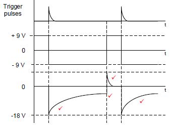
2.3
2.3.1 R1 & R2. ✓ (1)
2.3.2 The output will keep on oscillating between high and low states because both the trigger pin 2 and threshold pin 6 ✓ is connected to the top of the timing capacitor. ✓ (2)
2.3.3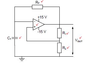
NOTE: The circuit connection must be correct before allocatingmarks to components.
The supplies should be indicated for the Op-amp to be accepted as correct. (6)
2.4
- The signal is fed into the inverting input of the Op-amp which acts as a comparator, comparing the voltages on its two input terminals. ✓
- The difference on the two input terminals drives the output of the Op-amp into one of its saturation states. ✓
- This output is divided across the two resistors RF and R1 into a fraction which is fed back to the non-inverting input. ✓
- The voltage on the non-inverting input determines (sets) the lower and upper trigger voltage levels. ✓
- The voltage on the inverting input is compared to the voltage on the noninverting input (trigger voltage level), if it’s lower than the trigger voltage
level, the output is driven into positive saturation. ✓ - If it is higher than the trigger voltage, it is driven into negative saturation.✓
(6)
2.5
2.5.1 A summing amplifier is used to add two or more different input signals ✓ to create one amplified output signal. ✓ (2)
2.5.2 VOUT=-(V₁+V₂+V₃)
=-(0,5+1,2+0,9)
=-2,6v
OR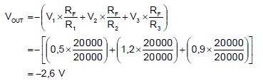
2.5.3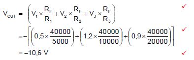
2.5.4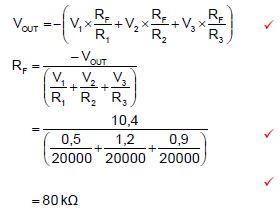
OR
RF=AV x RIN
=4 x 20000
=80000Ω
=80kΩ
NOTE: A resistance cannot be negative, that is the reason why the negative sign is omitted in the substitution stage. The negative sign only shows inversion of the output signal.
2.5.5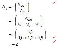
(3)
2.6
2.6.1
A – Passive RC differentiator. ✓
B – Passive RC integrator. ✓ (2)
2.6.2
With a long time constant the left hand plate of the capacitor immediately charges up to positive potential, ✓ thereafter the right hand plate slowly discharges ✓ and before it is completely discharged the polarity of the input swings to the opposite potential.✓ The capacitor then immediately charges to negative potential again and the process repeats itself. (3)
2.6.3
To convert ✓ square waves into triangular waves ✓
To change the shape of one type of wave to another wave. (2)
2.7
2.7.1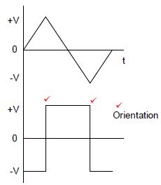
NOTE: The trigger points are only accepted if the wave shape is
correct.
1 mark for correct orientation if the wave shape is correct (3)
2.7.2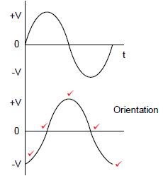
NOTE: The trigger points are only accepted if the wave shape is
correct.
1 mark for correct orientation if the wave shape is correct (5)
2.7.3
- The input and output impedance is improved✓
- Gain is boosted ✓
- Circuit is more stable. (2)
[60]
QUESTION 3: SEMICONDUCTOR DEVICES
3.1
Infinite gain.✓
Infinite input impedance.✓
Zero output impedance.✓
Infinite Bandwidth.✓
Infinite common mode rejection ratio.
Unconditional stability. (4)
3.2
3.2.1
=1 + 50000/10000
=6
(3)
3.2.2![]()
=1,5 x (1 + 50000/10000)
=9V
(3)
3.2.3 If the value of the feedback resistor is decreased the gain of the amplifier will decrease✓ causing the output voltage to decrease. ✓ (2)
3.3
3.3.1 Pin 2 = Trigger input.✓ (1)
3.3.2 This pin sets the voltage at which the 555 IC will trigger. It is used to maintain ✓ the voltage across the timing capacitor ✓ which is discharged through pin 7. ✓ (3)
3.3.3 The 555 IC can operate from power supply voltages of between +5 V ✓ and +18 V. ✓ (2)
3.3.4 In this mode the 555 timer is astable ('free running'), therefore its output will continuously toggle between High and Low ✓ thus generating a continuous train of square-wave pulses. ✓ (2)
[20]
QUESTION 4: DIGITAL AND SEQUENTIAL DEVICES
4.1
Liquid Crystal display (LCD) ✓
Light emitting diode (LED) ✓ (2)
4.2 The anodes of all the LEDs are connected together ✓on the positive voltage rail.✓ (2)
4.3 Current sinking ✓ digital output. (1)
4.4
Light waves travel naturally in both horizontal and vertical planes ✓ but when passed through a grid that only allows a single plane of light to pass ✓ while all
other light planes are stopped, ✓ the light is said to be polarised.
Polarisation of light is when the light passes through a filter which allows only a single plane of light to pass through and blocks the other planes of light. (3)
4.5
4.5.1 Decoder ✓ (1)
4.5.2
| Inputs | Outputs | ||||
| A | B | 0 | 1 | 2 | 3 |
| 0 | 0 | 1 | 0 | 0 | 0 |
| 0 | 1 | 0 | 1 | 0 | 0 |
| 1 | 0 | 0 | 0 | 1 | 0 |
| 1 | 1 | 0 | 0 | 0 | 1 |
(3)
4.6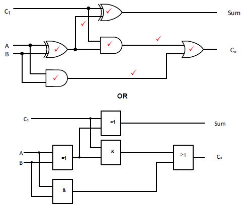
4.7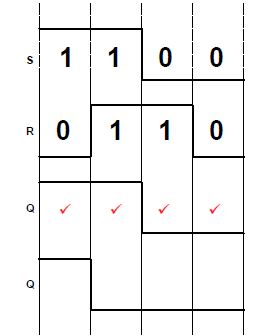 (4)
(4)
4.8
| MODE OF OPERATION | INPUTS | OUTPUTS | |||
| CLK | J | K | Q | ||
| HOLD | | 0 | 0 | No Change | |
RESET | | 0 | 1 | 0 | 1 |
SET | | 1 | 0 | 1 | 0 |
TOGGLE | | 1 | 1 | Change to Opposite state | |
(4)
4.9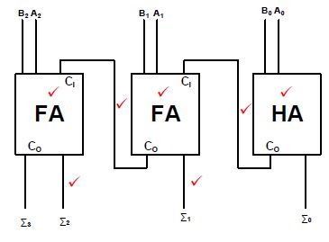 (7)
(7)
4.10
Asynchronous✓/ Ripple
Synchronous✓
Up/down
Down
Self-stopping
Decade / BCD(2)
4.11
Combinational logic circuits use AND, OR and NOT gates (logic gates) ✓ as their basic elements.
Sequential logic circuits rely on the flip-flop ✓ as its basic building elements. (2)
4.12
4.12.1 Three-bit synchronous down counter. ✓ (1)
4.12.2
| CLOCK PULSES | BINARY COUNT SEQUENCE | ||
| C | B | A | |
| 0 | 0 | 0 | 0 |
| 1 | 1 | 1 | 1 |
| 2 | 1 | 1 | 0 |
| 3 | 1 | 0 | 1 |
| 4 | 1 | 0 | 0 |
| 5 | 0 | 1 | 1 |
| 6 | 0 | 1 | 0 |
| 7 | 0 | 0 | 1 |
| 8 | 0 | 0 | 0 |
(6)
4.13
Serial – in : Parallel – out shift register (SIPO) ✓
Parallel – in : Serial – out shift Register (PISO) ✓
Parallel – in : Parallel – out shift Register (PIPO) (2)
4.14
4.14.1
A = Serial data in✓
B = Clock✓ (2)
4.14.2
The bits are loaded into the register one bit at a time ✓ usually from the left, ✓ moving the data from one flip-flop to the next flip flop ✓ for every clock pulse. ✓ This register will require 4 clock pulses to shift four bits in and 4 clock pulses to shift four bits out of the register. ✓
For example, a four-bit number such as 1111 will need four clock pulses to be loaded into the register and another four clock pulses for the number to move out in a serial manner. (5)
[55]
QUESTION 5: MICROCONTROLLERS
5.1
5.1.1 Microcontroller ✓ (1)
5.1.2 ROM - Read Only memory. ✓ (1)
5.1.3 Random Access Memory. ✓ (1)
5.1.4 This is a fast, temporary memory that allows information to be stored ✓ and retrieved by the system as it operates. ✓ (2)
5.2
5.2.1
Discrete logic consists of a single processor ✓ with many separate logic chips. ✓
Discrete logic is a term that refers to logic circuits that consists of many separate logic components. (2)
5.2.2 Integrated logic consists of the entire processor ✓ on a single chip. ✓ (2)
5.3
5.3.1
Memory Address Register (MAR) ✓
Memory Data Register (MDR)
Current Instruction Register (CIR)
Program counter (1)
5.3.2 The accumulator stores data ✓ that is needed for any arithmetic operation. ✓ (2)
5.4
5.4.1 It is used to pass information, data and instructions ✓ between the respective parts of the microcontroller ✓ as well as to communicate with the 'outside world' through input and output ports. ✓ (3)
5.4.2
Control bus ✓
Data bus ✓
Address bus ✓ (3)
5.4.3
Supports a higher data transfer rate. ✓
The sender and the receiver uses the same clock pulse. ✓ (2)
5.4.4
Requires more communication lines. ✓
Requires more space. ✓
Requires larger connections. (2)
5.5
5.5.1 A UART converts parallel data ✓ from the host processor ✓ into a serial data stream. ✓ (3)
5.5.2
Serial Peripheral Interface (SPI) ✓
Inter-Integrated Bus (I2C) ✓ (2)
5.6
5.6.1
Logic '1' = less than -200 mV ✓
Logic '0' = greater than +200 mV ✓ (2)
5.6.2
To connect the following to the main frame:
Point of sale terminals. ✓
Metering instruments. ✓
Large special automated machines. ✓ (3)
5.6.3
Simplex data communication is where all data and information travels in only one direction ✓ from transmitter to receiver. ✓
Half duplex communication is where the two devices take turn in communicating, ✓ one after the other. ✓ (4)
5.7
5.7.1 A program is a sequence of instructions ✓ that tells a computer to perform a task. ✓ (2)
5.7.2 A flow diagram is a visual representation of the sequence of steps and decisions ✓ needed to perform and complete a process. ✓ (2)
5.7.3 Debugging is the process of identifying ✓ and removing ✓ errors. (2)
5.8
5.8.1 Process element ✓ (1)
5.8.2 Data element ✓ (1)
5.8.3 Decision element ✓ (1)
5.9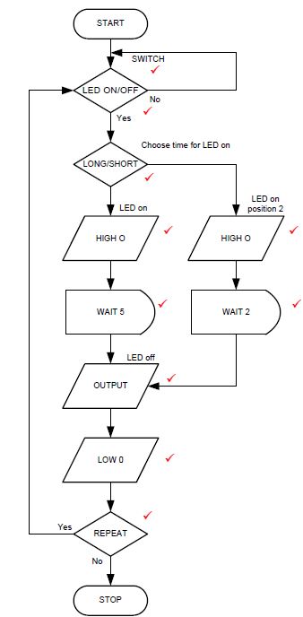
NOTE: If a Yes/No is indicated at the correct place, a maximum of 1 mark is allocated for the Yes/No decisions. (10)
OR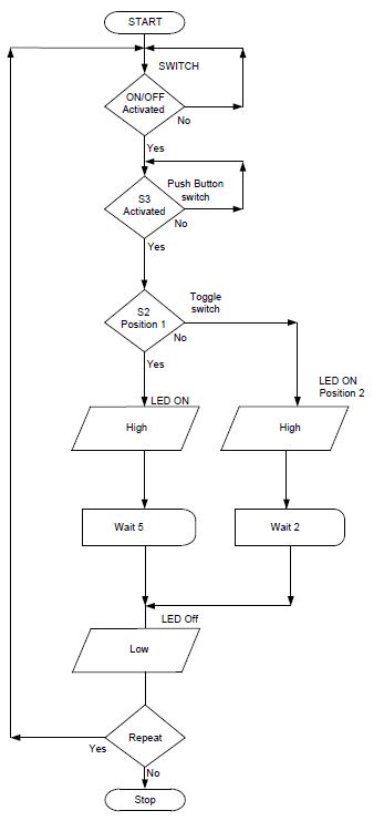
[55]