ELECTRICAL TECHNOLOGY (DIGITAL) GRADE 12 QUESTIONS - NSC EXAMS PAST PAPERS AND MEMOS MAY/JUNE 2021
Share via Whatsapp Join our WhatsApp Group Join our Telegram GroupELECTRICAL TECHNOLOGY (DIGITAL)
GRADE 12
NATIONAL SENIOR CERTIFICATE EXAMINATIONS
MAY/JUNE 2021
INSTRUCTIONS AND INFORMATION
- This question paper consists of FIVE questions.
- Answer ALL the questions.
- Answer the following questions on the attached ANSWER SHEETS:
QUESTIONS 2.2.4, 2.7.1 and 2.7.2
QUESTIONS 4.5.2, 4.6, 4.7, 4.8, 4.9 and 4.12.2
QUESTION 5.9 - Write your CENTRE NUMBER and EXAMINATION NUMBER on every ANSWER SHEET and hand them in with your ANSWER BOOK, whether you have used them or not.
- Sketches and diagrams must be large, neat and FULLY LABELLED.
- Show ALL calculations and round off answers correctly to TWO decimal places.
- Number the answers correctly according to the numbering system used in this question paper.
- You may use a non-programmable calculator.
- Calculations must include:
9.1.Formulae and manipulations where needed
9.2 Correct replacement of values
9.3 Correct answer and relevant units where applicable - A formula sheet is attached at the end of this question paper.
- Write neatly and legibly.
QUESTION 1: OCCUPATIONAL HEALTH AND SAFETY
1.1 Define the term safe with reference to the Occupational Health and Safety (1)
Act, 1993 (Act 85 of 1993).
1.2 State TWO characteristics or moral principles related to work ethics. (2)
1.3 Give ONE category/example of a dangerous practice in a workshop. (1)
1.4 Explain why poor ventilation is an unsafe condition in a workshop. (2)
1.5 Name TWO general duties of employees at the workplace. (2)
1.6 Explain the need for human rights in the workplace. (2)
[10]
QUESTION 2: SWITCHING CIRCUITS
2.1 Refer to FIGURE 2.1 below and answer the questions that follow.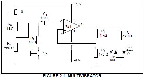
2.1.1 Identify the multivibrator in FIGURE 2.1. (1)
2.1.2 State the polarity of the pulse provided on the inverting input when switch S1 is pressed. (1)
2.1.3 State TWO functions of the 741 op amp in the circuit. (2)
2.1.4 Which LED will be forward biased when S1 is pressed? (1)
2.1.5 State the polarity of the voltage present on pin 3 after switch S2 is pressed. (1)
2.2 FIGURE 2.2 below shows a 741 op-amp monostable multivibrator. Answer
the questions that follow.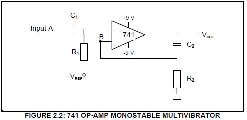
2.2.1 Write down the value of the voltage across capacitor C2 when the circuit is in its natural resting position. (1)
2.2.2 Write down the voltage at point B when the circuit is in its reset state. (1)
2.2.3 Explain when the circuit output will change state. (2)
2.2.4 On the ANSWER SHEET for QUESTION 2.2.4, draw the voltage at point B if the input signal below is applied to the input of the circuit.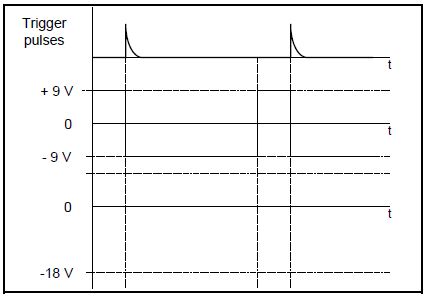
2.3 Refer to the multivibrator in FIGURE 2.3 below and answer the questions that follow.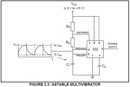
2.3.1 Identify the components responsible for charging capacitor C1. (1)
2.3.2 Explain why the output will keep oscillating between high and low states. (2)
2.3.3 Draw a fully labelled 741 IC op-amp equivalent of the circuit in FIGURE 2.3. (6)
2.4 Explain the operation of the circuit in FIGURE 2.4 below.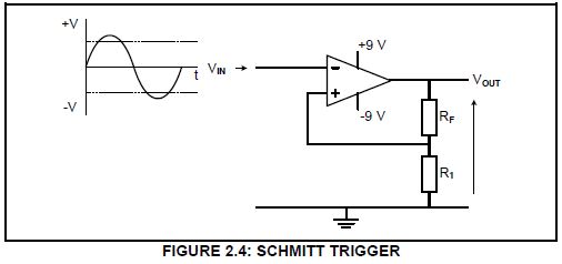
2.5 FIGURE 2.5 and TABLE 2.5 below show the resistor values, output voltages and gain of a summing amplifier. Refer to FIGURE 2.5 and study TABLE 2.5 to answer the questions that follow.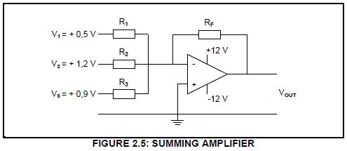
| RESISTOR VALUES | OUTPUT | GAIN | |||
| R1 | R2 | R3 | RF | VOUT | β (AV) |
| 20 kΩ | 20 kΩ | 20 kΩ | 20 kΩ | B | 1 |
| 20 kΩ | 20 kΩ | 20 kΩ | 40 kΩ | + 5,2 V | D |
| 5 kΩ | 10 kΩ | 20 kΩ | 40 kΩ | C | 4,08 |
| 20 kΩ | 20 kΩ | 20 kΩ | A | + 10,4 V | 4 |
TABLE 2.5
2.5.1 State the function of a summing amplifier. (2)
2.5.2 Calculate the output voltage at B. (3)
2.5.3 Calculate the output voltage at C. (3)
2.5.4 Calculate the value of the feedback at A. (3)
2.5.5 Calculate the total gain at D. (3)
2.6 Refer to FIGURE 4.6 below and answer the questions that follow.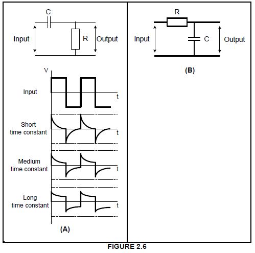
2.6.1 Identify the circuits in FIGURE 4.6(A) and (B). (2)
2.6.2 Explain the effect that a long time constant has on the operation of the circuit in FIGURE 4.6(A). (3)
2.6.3 Explain the function of the circuit in FIGURE 4.6(B). (2)
2.7 Refer to FIGURE 2.7 below and answer the questions that follow.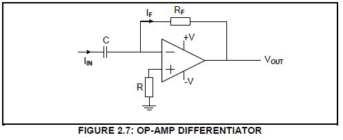
On the ANSWER SHEET for QUESTION 2.7.1 and QUESTION 2.7.2, draw the output waveform if the following inputs are applied to the circuit.
2.7.1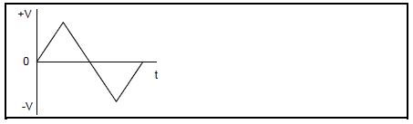
(3)
2.7.2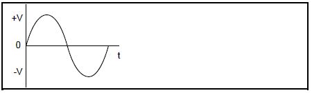
(5)
2.7.3 State TWO improvements that the op amp brings to the operation of the circuit in FIGURE 2.7. (2)
[60]
QUESTION 3: SEMICONDUCTOR DEVICES
3.1 Name FOUR characteristics of an ideal operational amplifier. (4)
3.2 FIGURE 3.2 below shows the op amp as a non-inverting amplifier. Answer the questions that follow.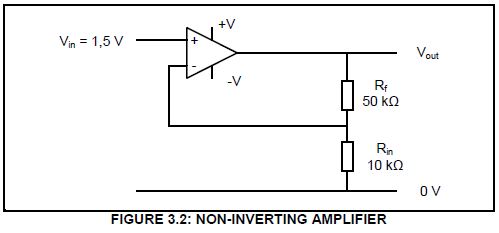
Given
VIN= 1,5V
RF=50 kΩ
RIN=10 kΩ
3.2.1 Calculate the voltage gain in FIGURE 3.5. (3)
3.2.2 Calculate the output voltage. (3)
3.2.3 Describe the effects of decreasing the feedback resistor. (2)
3.3 FIGURE 3.3 below shows the 555 timer IC. Answer the questions that follow.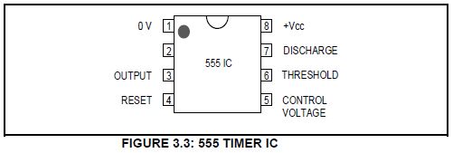
3.3.1 Identify pin 2. (1)
3.3.2 Explain the function of pin 6 (threshold) on a 555 IC. (3)
3.3.3 State the voltage parameters between which a 555 timer can operate. (2)
3.3.4 Explain the astable mode of operation of a 555 timer. (2)
[20]
QUESTION 4: DIGITAL AND SEQUENTIAL DEVICES
4.1 Name TWO methods to display information in digital systems. (2)
4.2 Explain the term common anode with reference to the seven-segment LED display. (2)
4.3 Refer to transistor coupling as used in LED seven-segment displays and identify the circuit in FIGURE 4.3 below. (1)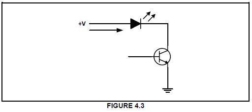
4.4 Explain the term polarisation of light with reference to liquid crystal display (LCD). (3)
4.5 Refer to FIGURE 4.5 below and answer the questions that follow.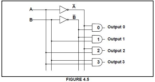
4.5.1 Identify the circuit in FIGURE 4.5. (1)
4.5.2 Complete the truth table of FIGURE 4.5 on the ANSWER SHEET for QUESTION 4.5.2. (3)
4.6 On the ANSWER SHEET for QUESTION 4.6, draw the logic circuit of a full adder using AND gates, exclusive OR gates and an OR gate. (8)
4.7 FIGURE 4.7 below shows a clocked RS flip-flop. Complete the output waveforms on the ANSWER SHEET for QUESTION 4.7.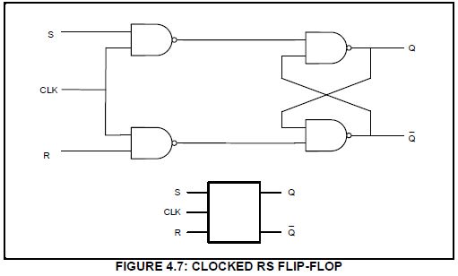
FIGURE 4.7: CLOCKED RS FLIP-FLOP (4)
4.8 FIGURE 4.8 below shows the logic symbol of a clocked J-K flip flop. Complete the truth table of this flip-flop on the ANSWER SHEET for QUESTION 4.8.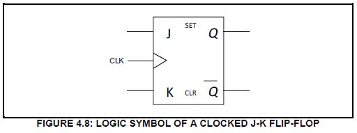
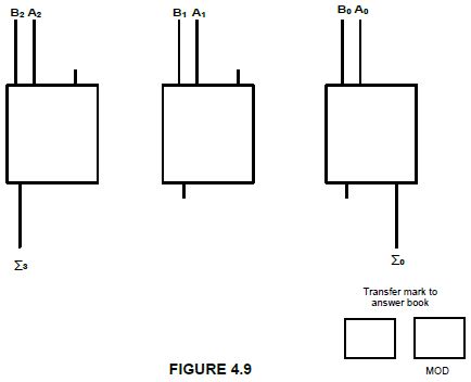
4.9 On the ANSWER SHEET for QUESTION 4.9, draw the circuit of a three-bit parallel adder which will add two three-bit numbers to produce a single threebit number as well as a carry-over bit. (7)
4.10 Name TWO types of counters that are commonly used in digital electronics. (2)
4.11 Explain the difference between combinational logic circuits and sequential logic circuits with regard to their basic building elements. (2)
4.12 Refer to FIGURE 4.12 below and answer the questions that follow.
4.12.1 Identify the counter in FIGURE 4.12. (1)
4.12.2 On the ANSWER SHEET for QUESTION 4.12.2, complete the truth table of this counter. (6)
4.13 Name TWO types of shift registers, other than the serial-in: serial-out shift register, that are used in digital electronic circuits. (2)
4.14 Refer to FIGURE 4.14 below which is a block diagram of a serial-in: serial-out shift register and answer the questions that follow.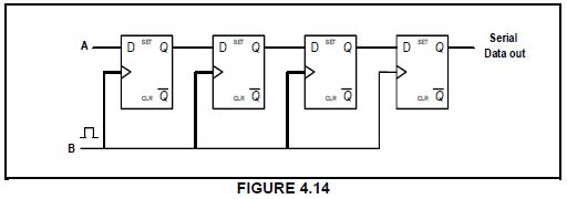
4.14.1 Label A and B. (2)
4.14.2 Explain the operation of this register. (5)
[55]
QUESTION 5: MICROCONTROLLERS
5.1 Refer to the block diagram in FIGURE 5.1 below and answer the questions that follow.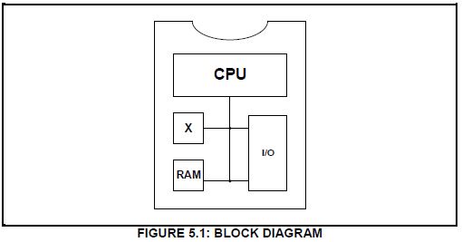
5.1.1 Identify the block diagram in FIGURE 5.1. (1)
5.1.2 Identify component X. (1)
5.1.3 Write out the abbreviation RAM in full. (1)
5.1.4 Explain the function of the RAM. (2)
5.2 Refer to the hardware of a microcontroller and answer the questions that follow.
5.2.1 Explain the term discreet logic. (2)
5.2.2 Explain the term integrated logic. (2)
5.3 Refer to the registers of a CPU and answer the questions that follow.
5.3.1 Name ONE type of special-purpose register. (1)
5.3.2 Describe the function of an accumulator. (2)
5.4 Refer to communication in a microcontroller and answer the questions that follow.
5.4.1 Explain the function of the system bus. (3)
5.4.2 Name the THREE busses in a microcontroller. (3)
5.4.3 State TWO advantages of synchronous communication when compared to asynchronous communication. (2)
5.4.4 State TWO disadvantages of parallel communication when compared to serial communication. (2)
5.5 Refer to communication peripherals and answer the questions that follow.
5.5.1 Explain the function of the universal asynchronous receiver transmitter (UART). (3)
5.5.2 Name TWO communication peripherals other than the universal asynchronous receiver transmitter (UART). (2)
5.6 Refer to RS-485 communication protocol and answer the questions that follow.
5.6.1 State the operating voltages for logic '1' and logic '0'. (2)
5.6.2 State THREE applications of the RS-485. (3)
5.6.3 Explain the differences between simplex communication and half duplex communication. (4)
5.7 Define the terms below with reference to the software of microcontrollers:
5.7.1 Program (2)
5.7.2 Flow diagram (2)
5.7.3 Debugging (2)
5.8 Identify the following flow diagram symbols in PICAXE:
5.8.1 
(1)
5.8.2 
(1)
5.8.3 
(1)
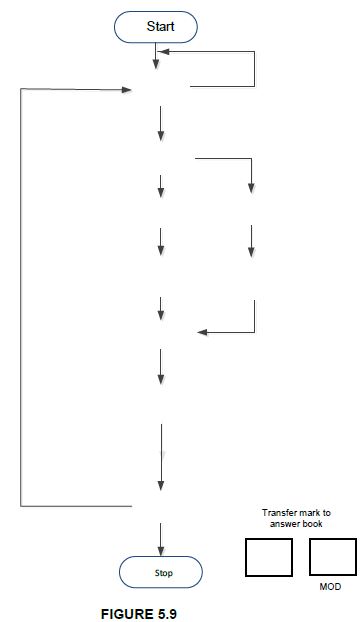
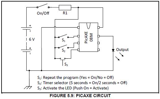
5.9 Study the PICAXE circuit in FIGURE 5.9 below and design a flow diagram for the circuit. Complete your answer on the ANSWER SHEET for QUESTION 5.9.
SCENARIO:
When the on/off switch is activated the program must execute as follows:
- S3 must be pushed to activate the OUTPUT LED (the LED will come on for either 5 or 2 seconds). S3 is a push-button.
- S2 must be used to select one of TWO timers (one set to 5 seconds and the other to 2 seconds). S2 is a toggle switch.
- S1 must allow the user to repeat the program or to stop it. S1 is a toggle switch.
FORMULA SHEET
SEMICONDUCTOR DEVICES |
SWITCHING CIRCUITS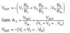 |
| CENTRE NUMBER: |
| EXAMINATION NUMBER: |
ANSWER SHEET
QUESTION 2: SWITCHING CIRCUITS
2.2.4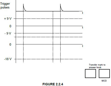
| CENTRE NUMBER: |
| EXAMINATION NUMBER: |
ANSWER SHEET
2.7.1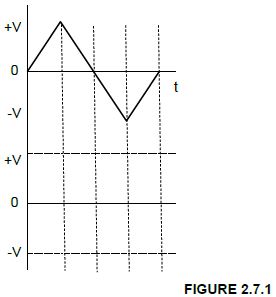
2.7.2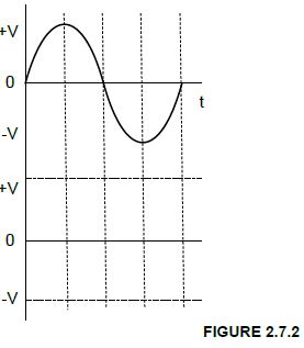
| CENTRE NUMBER: |
| EXAMINATION NUMBER: |
ANSWER SHEET
QUESTION 4: DIGITAL AND SEQUENTIAL DEVICES
4.5.2
| Inputs | Outputs | ||||
| A | B | 0 | 1 | 2 | 3 |
| 0 | 0 | 1 | 0 | 0 | 0 |
| 0 | 1 | 0 | 1 | 0 | |
| 1 | 0 | 0 | 0 | 1 | |
| 1 | 1 | 0 | 0 | 0 | |
4.6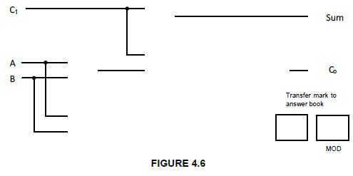
| CENTRE NUMBER: |
| EXAMINATION NUMBER: |
ANSWER SHEET
4.7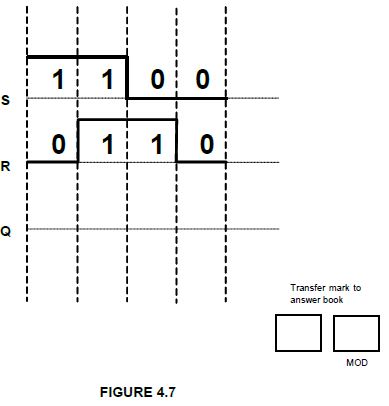
| CENTRE NUMBER: |
| EXAMINATION NUMBER: |
ANSWER SHEET
4.8
| MODE OF OPERATION | INPUTS | OUTPUTS | |||
| CLK | J | K | Q | ||
| HOLD | | 0 | 0 | No Change | |
RESET | | 0 | 1 | ||
SET | | 1 | 0 | ||
TOGGLE | | 1 | 1 | Change to Opposite state | |
TABLE 4.8
4.9
| CENTRE NUMBER: |
| EXAMINATION NUMBER: |
ANSWER SHEET
4.12.2
| CLOCK PULSES | BINARY COUNT SEQUENCE | ||
| C | B | A | |
| 0 | 0 | 0 | 0 |
| 1 | 1 | 1 | 1 |
| 2 | 1 | 1 | |
| 3 | 1 | 0 | |
| 4 | 0 | 0 | |
| 5 | 0 | 1 | |
| 6 | 0 | 1 | |
| 7 | 0 | 0 | 1 |
| 8 | 0 | 0 | |
TABLE 4.12.2
| CENTRE NUMBER: |
| EXAMINATION NUMBER: |
ANSWER SHEET