ELECTRICAL TECHNOLOGY(ELECTRONICS) GRADE 12 MEMORANDUM - NSC PAST PAPERS AND MEMOS NOVEMBER 2019
Share via Whatsapp Join our WhatsApp Group Join our Telegram GroupELECTRICAL TECHNOLOGY: ELECTRONICS
GRADE 12
NATIONAL SENIOR CERTIFICATE
MEMORANDUM
NOVEMBER 2019
INSTRUCTIONS TO THE MARKERS
- All questions with multiple answers imply that any relevant, acceptable answer should be considered.
- Calculations:
2.1 All calculations must show the formulae.
2.2 Substitution of values must be done correctly.
2.3 All answers MUST contain the correct unit to be considered.
2.4 Alternative methods must be considered, provided that the correct answer is obtained.
2.5Where an incorrect answer could be carried over to the next step, the first answer will be deemed incorrect. However, should the incorrect answer be carried over correctly, the marker has to re-calculate the values, using the incorrect answer from the first calculation. If correctly used, the candidate should receive the full marks for subsequent calculations.
2.6 Markers should consider when and where a candidate has rounded off in a calculation, as well as the subsequent effect it has on the final answer obtained. The calculation should therefore be awarded marks on merit. - These marking guidelines are only a guide with model answers. Alternative interpretations must be considered and marked on merit. However, this principle should be applied consistently throughout the marking session at ALL marking centres.
QUESTION 1: OCCUPATIONAL HEALTH AND SAFETY
1.1
- An employee with a sense of teamwork helps a team to meet its goals.
- Teamwork helps a team deliver quality work.
- Teamwork can win the respect of your co-workers.
- Working together as a team can improve discipline in the workshop.
- Teamwork will lead to improved productivity. (2)
1.2
1.2.1 The purpose of the Act is to:
- Provide for health and safety of persons at work.
- Protect against hazards arising from the activities of other people at work.
- Establish an advisory council for occupational health and safety and related matters.
- Provide for health and safety for persons in connection with the use of plant and machinery (2)
1.2.2 Workplace can be defined as any premises or place where a person performs work ü during the time of his employment. (2)
1.3
1.3.1 Employee. Learner, Supervisor, Team leader, Safety representative (1)
1.3.2 Health and safety representative. ü Inspector. (1)
1.4
- Remain calm.
- Stop whatever you are doing.
- Switch off machinery.
- Notify a responsible adult or teacher.
- If there is an emergency stop nearby activate it if necessary.
- Move in an orderly manner to the nearest assembly point.
NOTE: Procedure can be listed in any order (2)
[10]
QUESTION 2: RLC CIRCUITS
2.1
2.1.1 Power factor is the ratio of the true power to the apparent power.
NOTE: If the formula is written 1 mark must be awarded (2)
2.1.2 The quality factor of an inductor refers to the ratio of the inductor's reactance to its internal resistance during resonance.
If the formula is written 1 mark must be awarded
The ratio of the inductive/capacitive voltage to the supply voltage during resonance
The ratio of the inductive/capacitive reactance to the impedance during resonance (2)
2.2
- Wattless voltage dividers
- Timing circuits
- Filter circuits
- Oscillating circuits
- Radio-tuning circuits (2)
2.3
2.3.1 VT = √VR2 + (VC - VL)2
= √122 + (24 - 16)2
= 14.42V (3)
2.3.2 XL = V L
I
= 16
3
= 5.33Ω (3)
2.3.3 The circuit is capacitive because the voltage drop across the capacitor is greater than the voltage across the inductor.
NOTE: If XL and XC are calculated and stated as a capacitive circuit, 2 marks should be awarded.
If the learner wrote, the circuit is inductive, but give the same reason, that motivation is deemed incorrect.(2)
2.3.4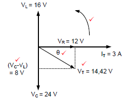
NOTE: No label, no marks (4)
2.3.5 When the impedance of the circuit is increased, the power factor will decrease therefore increasing the value of the phase angle. (2)
2.4
2.4.1 IT = √IR2 +(IL - Ic)2
= √62 +(4 - 3)2
= 6.08A (3)
2.4.2
Cosθ = I R
IT
θ = Cos-1 6
6.08
= 9.30 (3)
2.4.3 The phase angle is lagging because the inductive current is larger than the capacitive current.
NOTE: If only the second part of the answer is given = 1 mark (2)
2.5
2.5.1 At resonance XL = XC = 50 Ω
C = 1
2πfXc
= 1
2 x π x 2000 x 50
= 1.59µF (4)
NOTE: If the learner only substituted 50 Ω in the place of XC, the correct substitution will be awarded 2 marks
If the learner calculated the inductance first, and used the resonant frequency’s formula to work out the capacitance full marks must be awarded.
L= XL
2 × πf
L= 50
2×π×(2000)
L= 3,98×10⁻³H
fr= 1
2π√LC
2000= 1
2π√3.97 x 10⁻³ x C
2000(2π√3.97 x 10⁻³ x C) = 1
C = 1.6μF
2.5.2 At resonance R = Z = 12Ω
I = VT
Z
= 120
12
= 10A (4)
If R is used in the place of Z, full marks are awarded
2.5.3 If the resistance is doubled, the current will be halved. (1)
2.5.4 Z = R
VL = VC
VR = VT
XL = XC
Cosθ = 1
θ = 0º
I = maximum
Z = minimum (3)
[40]
QUESTION 3: SEMICONDUCTOR DEVICES
3.1 N-type semiconductor material. (1)
3.2 N-channel JFET.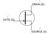
NOTE: The symbol must be drawn correctly to receive marks for labelling. (3)
3.3
3.3.1 P-channel. (1)
3.3.2 The drain must be connected to positive.
The source must be connected to negative.
The gate voltage must be positive. (3)
3.4
3.4.1 Switch
Oscillators
Phase Control circuits
Timing circuits (1)
3.4.2 The UJT triggers when the voltage across the capacitor / emitter rises to 0,7 V above the intrinsic standoff ratio (VX or VBB).
The UJT triggers on when the voltage across the capacitor / emitter rises to the UJT's peak voltage VP. (2)
3.4.3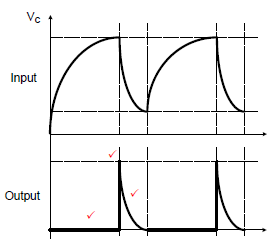
(3)
3.5
3.5.1 Pin 1 is identified by being the first pin to the left and below the indentation.
OR
Being closest to the dot in the body of the IC. (1)
3.5.2 Input stage or differential amplifier
Intermediate stage üor high gain differential amplifier
Output stage or common collector (3)
3.6
3.6.1
(3)
3.6.2 The amplifier is driven into saturation which causes the tops and bottoms to be clipped.
If the learner identified that the input is fed into the inverting input, there will be a 180 degree phase shift on the output = 2 marks (2)
3.6.3 +15 volts –15 volts (2)
3.7
3.7.1 Dual in-line package (1)
3.7.2 16 V (1)
3.7.3 5 V (1)
3.8 When the trigger voltage rises above the threshold voltage, the output of a 555 timer will change state from high to low.
NOTE: If the answer is given as “Switch off” only = 1 mark (2)
[30]
QUESTION 4: SWITCHING CIRCUITS
4.1
4.1.1
- – Bistable multivibrator
- – Monostable multivibrator (2)
4.1.2 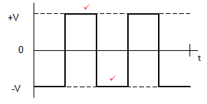
2 marks = 1 mark for each correct half cycle
If waveform is drawn correctly, but inverted, 2 marks will be awarded
NOTE: Due to the +V instead of -V typo on the answer sheet, the following responses are also accepted. (2)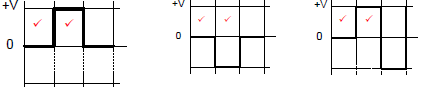
4.2
4.2.1 Resistors R1 and R2 are pull-up resistors.
R1 and R2 hold both trigger pin 2 and reset pin 4 high. (2)
4.2.2 When set switch S1 is pressed, trigger pin 2 will be pulled low and cause the IC output to 'flip' and rise high turning the LED on. (3)
4.2.3 Threshold pin 6 is purposefully held at 0 V causing the IC not to reset, keeping the output high when S1 is pressed, (3)
4.3
4.3.1 The output signal represents an inverting Schmitt trigger ü because the output signal is inverted with reference to the input signal.
OR
The output signal is at -VCC when triggered by the upper trigger voltage and swings to +VCC when triggered by the lower trigger voltage.(3)
4.3.2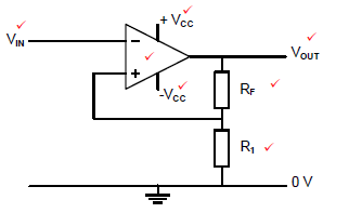
NOTE: Where a portion of the circuit is incorrect, he/she will lose those marks and will be awarded marks for the correct section / labels.
Any 7 correct labels (7)
4.4
4.4.1 Inverting comparator (2)
4.4.2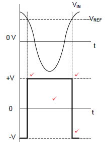
1 mark = inversion
1 mark = correct wave shape
2 marks = 1 mark for each correct trigger point. (4)
4.4.3 Change the connection of resistor R1 from the positive supply to the negative supply. (2)
4.5
4.5.1 The gain of the amplifier is determined by the ratio of the feedback resistance ü to the input resistance of each branch.
NOTE: Writing the formula only = 1 mark. (3)
4.5.2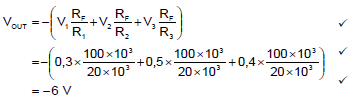
NOTE: If the – sign is omitted in the answer, it is incorrect because it is an inverted summing amplifier. (3)
4.5.3
The amplifier is not saturated because the output voltage is less ü than the supply voltage. (2)
4.5.4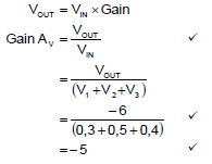
(3)
4.5.5 With a variable resistor in the feedback loop, the gain ü of the amplifier can be varied / controlled. (2)
4.5.6 If R2 is changed to 10 kΩ, the gain for V2 will increase ü causing the total output voltage to increase. (2)
4.6
4.6.1 RC passive differentiator
NOTE: RC circuit = 1mark (2)
4.6.2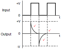
1 mark = positive pulse
1 mark = negative pulse
1 mark = correct orientation (3)
4.6.3 If the circuit time constant is increased, the capacitor will discharge slower ü producing a sagging square wave.
NOTE: If the learner draws the waveform and label correctly, mark on merit. (2)
4.7
4.7.1 CF provides a feedback connection from output to input. (1)
4.7.2 The inputs draw zero current.
The two inputs will have the same voltage at all times.
The capacitor will charge at a constant rate when a constant current is supplied.
NOTE: If the learner gives a correct account of the operation of the integrator as applied with the 741 op-amp, the answer must be marked on merit. (3)
4.7.3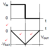
2 marks = correct labelling
2 marks = 1 mark for each correct half cycle
NOTE: The wave must be drawn correct before marks can be awarded for labelling. (4)
[60]
QUESTION 5: AMPLIFIERS
5.1
5.1.1 Q Point
Class A Amplifier - The Q point is in the middle of the DC load line.
Class B Amplifier - The Q point is on the cut-off of the DC load line.
NOTE: If a learner draws the Q point instead of a narrative answer, mark on merit (2)
5.1.2 Efficiency
Class A Amplifier - It has low efficiency therefore it has less output power.
Class B Amplifier - It has higher efficiency therefore produces more output power.
Class A Amplifier - 25%
Class B Amplifier - 50% (2)
5.2
5.2.1 To limit the current flowing through the collector.
Protects the circuit from damage.
To protect the transistor. (1)
5.2.2 When the transistor is OFF, no collector current flows through it, therefore the maximum supply voltage will appear across the transistor.
OR
From the formula VCC = VCE + ICRC
If IC = 0 then
(ICRC= 0) therefore
( VCC= VCE) (2)
5.3 In Class C amplification, a transistor is biased below the cut off region therefore the collector current flows for less than 180°. (2)
5.4
5.4.1 Class A amplifier.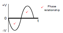
1 mark = phase relationship
2 marks = 1 mark for each correct half cycle (3)
5.4.2 Class AB amplifier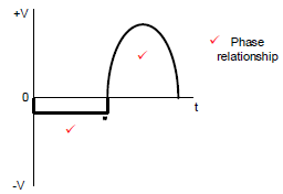
1 mark = phase relationship
2 marks = 1 mark for each correct half cycle (3)
5.5
- It can lead to the increases in currents leading to thermal runaway, which could destroy the transistor.
- Crossover point distortion may occur.
- Incorrect placement of the Q-point
- Non-linear amplification (Distortion)
- Changes in the power supply voltage can cause the transistor's currents to change.
NOTE: Bullet 5 is not an undesirable condition, but will be accepted because it is stated in the prescribed textbook. (1)
5.6
5.6.1 The emitter is common ü to both the input and the output circuits. (2)
5.6.2 Input signal will be connected between point B and C.
The load can be connected between point E and F. (2)
5.6.3 Emitter capacitor (CE)
Emitter resistor (RE) (2)
5.6.4 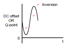
1 mark = inversion
2 marks = 1 mark for each amplified half cycle (3)
5.6.5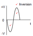
1 mark = inversion
2 marks = 1 mark for each amplified half cycle (3)
5.7
- Impedance matching.ü
- Correct frequency response.ü
- DC isolation. (2)
5.8
5.8.1
AP = 10log10 POUT
PIN
= 10log101200
3015
= -4dB (3)
5.8.2
AV = 20log10VOUT
VIN
= 20log10 219
230
= -0.43dB (3)
5.9 The gain of an amplifier is the capability of an amplifier to increase the magnitude of the input signal without distortion.
Gain is the ratio of how much bigger or smaller the output signal will be bigger in comparison to the input signal. (2)
5.10
AV = AV1 x AV2 x AV3
= 10 x 15 x 20
= 3000 (3)
5.11
5.11.1 Complimentary - symmetry Push-pull Amplifier. (2)
5.11.2 Cross-over distortion is eliminated by biasing the two push pull transistors each into class AB mode.
Cross-over distortion is eliminated by biasing the two push pull transistors just above the cut-off region. (2)
5.11.3 The resistors are used for correct biasing (1)
5.11.4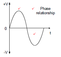
1 mark = phase relationship
2 marks = 1 mark for each amplified half cycle
NOTE: If the learner indicated cross-over distortion on the waveform, it will be accepted because of the two transistors used in the given circuit
If the frequency is wrong, the waveform is wrong. (3)
5.12
5.12.1 RC oscillator - Does not use a resonating tank circuit but uses selective resistors and capacitors in the feedback network.
LC oscillator - Uses tank circuit in the feedback network between the Drain and the Gate of the transistor. (2)
5.12.2 LC oscillators - The oscillating frequency is determined by the values of the capacitors and inductor in the tank circuit. (Colpitts oscillator)
OR
The oscillating frequency is determined by the values of the inductors and a capacitor in the tank circuit.(Hartley oscillator)
RC oscillator - the oscillating frequency is determined by the values of the resistors and the capacitors in the feedback circuit. (2)
5.13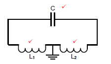
(3)
5.14 Provide a phase shift of 180 degrees.
Amplifies the signal from the tank circuit. (2)
5.15
Both their output waveforms are purely sinusoidal.
They both use a transistor for amplification.
They both use resistors for biasing.
They both use positive feedback to operate.
Both circuit’s feedback circuits creates a 180° phase shift.
Both circuit’s transistor configuration creates 180° phase shift. (2)
[60]
TOTAL: 200