ELECTRICAL TECHNOLOGY(ELECTRONICS) GRADE 12 QUESTIONS - NSC PAST PAPERS AND MEMOS NOVEMBER 2019
Share via Whatsapp Join our WhatsApp Group Join our Telegram GroupELECTRICAL TECHNOLOGY: ELECTRONICS
GRADE 12
NATIONAL SENIOR CERTIFICATE
NOVEMBER 2019
INSTRUCTIONS AND INFORMATION
- This question paper consists of FIVE questions.
- Answer ALL the questions.
- Answer the following questions on the attached ANSWER SHEETS:
QUESTIONS 2.1.2, 2.4.2, 2.6.2 and 2.7.3
QUESTIONS 4.2.2, 4.3.3, 4.4.2, 4.5.1 and 4.5.2 - Write your CENTRE NUMBER and EXAMINATION NUMBER on every ANSWER SHEET and hand them in with your ANSWER BOOK, whether you have used them or not.
- Sketches and diagrams must be large, neat and FULLY LABELLED.
- Show ALL calculations and round off answers correctly to TWO decimal places.
- Number the answers correctly according to the numbering system used in this question paper.
- You may use a non-programmable calculator.
- Calculations must include:
9.1 Formulae and manipulations where needed
9.2 Correct replacement of values
9.3 Correct answer and relevant units where applicable - A formula sheet is attached at the end of this question paper.
- Write neatly and legibly.
QUESTION 1: OCCUPATIONAL HEALTH AND SAFETY
1.1 Describe how teamwork improves work ethics. (2)
1.2 With reference to the Occupational Health and Safety Act, 1993 (Act 85 of 1993):
1.2.1 State TWO purposes of the Occupational Health and Safety Act, 1993 (Act 85 of 1993). (2)
1.2.2 Define the term workplace. (2)
1.3 An employer has a duty to report on occupational health and safety and related matters. Name ONE person they should inform when:
1.3.1 The allocated task is hazardous (1)
1.3.2 A major incident occurs (1)
1.4 State TWO general emergency procedures to be followed when the emergency siren is sounded at school. (2)
[10]
QUESTION 2: RLC CIRCUITS
2.1 Define the following with reference to RLC circuits:
2.1.1 Power factor (2)
2.1.2 Q-factor of an inductor in a resonant circuit (2)
2.2 State TWO applications of RLC circuits. (2)
2.3 FIGURE 2.3 below shows an RLC series circuit. Answer the questions that follow.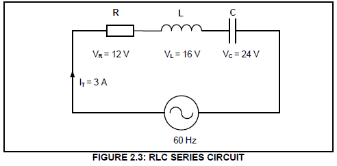
Given:
IT = 3 A
VR = 12 V
VL = 16 V
VC = 24 V
f = 60 Hz
2.3.1 Calculate the total voltage of the supply.(3)
2.3.2 Calculate the value of the inductive reactance.(3)
2.3.3 State if the circuit is capacitive or inductive. Motivate your answer.(2)
2.3.4 Complete the phasor diagram on the ANSWER SHEET for QUESTION 2.3.4 and show the direction of rotation.(4)
2.3.5 Describe how an increase in impedance, while keeping the resistance constant, will affect the phase angle and the power factor.(2)
2.4 FIGURE 2.4 below shows an RLC parallel circuit consisting of a 20 Ω resistor, an inductor with an inductive reactance of 30 Ω and a capacitor with a capacitive reactance of 40 Ω, all connected across a 120 V/60 Hz supply.
Answer the questions that follow.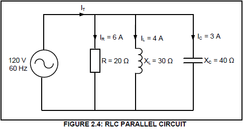
Given:
R = 20 Ω
XL = 30 Ω
XC = 40 Ω
VT = 120 V
f = 60 Hz
2.4.1 Calculate the total current in the circuit.(3)
2.4.2 Calculate the phase angle.(3)
2.4.3 State whether the phase angle is leading or lagging. Motivate your answer.(2)
2.5 FIGURE 2.5 below shows an RLC series resonant circuit which consists of a 12 Ω resistor, an inductor with an inductive reactance of 50 Ω and a variable capacitor, all connected across a 120 V/2 kHz supply. Answer the questions that follow.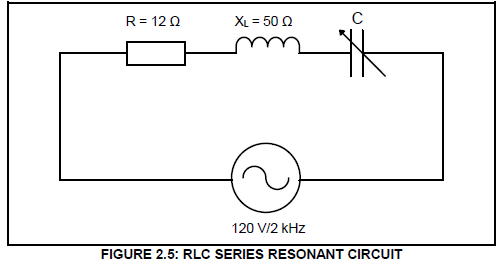
Given:
VT = 120 V
f = 2 kHz
R = 12 Ω
XL = 50 Ω
2.5.1 Calculate the value of C when the circuit resonates at 2 kHz.(4)
2.5.2 Calculate the value of the current in the circuit.(4)
2.5.3 State how current will be affected if the value of the resistance is doubled.(1)
2.5.4 List THREE characteristics of an RLC series circuit at resonance. (3)
[40]
QUESTION 3: SEMICONDUCTOR DEVICES
3.1 Name the type of material used for the gate terminal in a P-channel JFET. (1)
3.2 Draw a neatly labelled symbol of an N-channel JFET. (3)
3.3 Study the symbol in FIGURE 3.3 below and answer the questions that follow.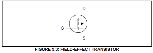
3.3.1 State whether the field-effect transistor (FET) in FIGURE 3.3 is a P-channel or an N-channel. (1)
3.3.2 List THREE conditions for the correct biasing of the transistor in FIGURE 3.3.(3)
3.4 Refer to FIGURE 3.4 below and answer the questions that follow.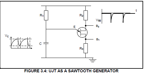
3.4.1 Besides a sawtooth generator, name ONE other application of a UJT (1)
3.4.2 Explain what causes the UJT to trigger ON in the circuit. (2)
3.4.3 Draw the output waveform between points B1 and ground on the ANSWER SHEET for QUESTION 3.4.3.(3)
3.5 Refer to FIGURE 3.5 below and answer the questions that follow.
3.5.1 State how you would identify pin 1 of the IC in FIGURE 3.5. (1)
3.5.2 List the THREE stages into which the internal circuit of the op-amp is divided. (3)
3.6 FIGURE 3.6 below shows the op-amp as an inverting amplifier. Answer the questions that follow.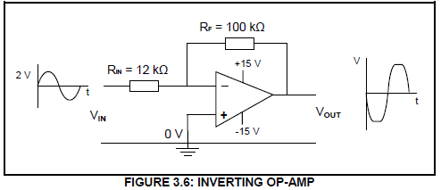
Given:
VIN = 2 V
RF = 100 kΩ
RIN = 12 kΩ
3.6.1 Calculate the output voltage based on the data in FIGURE 3.6. (3)
3.6.2 Explain why the shape of the output waveform is NOT an exact replica of the input waveform. (2)
3.6.3 Identify the maximum output voltages (Vout). (2)
3.7 Refer to the data sheet in FIGURE 3.7 below and answer the questions that follow.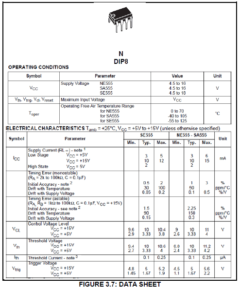
3.7.1 Rewrite the abbreviation DIP in full. (1)
3.7.2 Write down the maximum supply voltage for the NE555 IC (1)
3.7.3 Identify the typical trigger voltage of the NE555 IC, in the data sheet above, when the supply voltage is +15 V. (1)
3.8 Explain what will happen to the output of an NE555 IC when the trigger voltage rises above the threshold voltage level of 10 V. (2)
[30]
QUESTION 4: SWITCHING CIRCUITS
4.1 Refer to FIGURE 4.1 below and answer the questions that follow.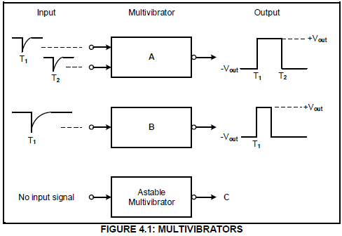
4.1.1 Identify multivibrators A and B. (2)
4.1.2 Draw the output signal of the astable multivibrator at C on the ANSWER SHEET for QUESTION 4.1.2 (2)
4.2 Refer to the circuit in FIGURE 4.2 below and answer the questions that follow.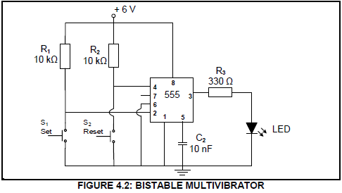
4.2.1 State the function of R1 and R2. (2)
4.2.2 Describe what happens when the set switch, S1, is pressed. (3)
4.2.3 Explain why threshold pin 6 is connected directly to ground. (3)
4.3 Refer to FIGURE 4.3 below and answer the questions that follow.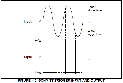
4.3.1 State whether the output signal represents an inverting or a non-inverting Schmitt trigger. Motivate your answer. (3)
4.3.2 Draw the circuit diagram of the Schmitt trigger consisting of two resistors and a 741 op-amp that will produce the output signal in FIGURE 4.3. (7)
4.4 Refer to FIGURE 4.4 below and answer the questions that follow.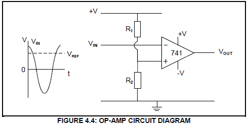
4.4.1 Identify the op-amp circuit diagram in FIGURE 4.4. (2)
4.4.2 Draw the output signal on the ANSWER SHEET for QUESTION 4.4.2 (4)
4.4.3 Explain how the reference voltage is made negative. (2)
4.5 Refer to FIGURE 4.5 below and answer the questions that follow.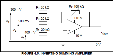
Given:
V1 = 300 mV
V2 = 500 mV
V3 = 400 mV
RF = 100 kΩ
R1 = R2 = R3 = 20 kΩ
4.5.1 Explain how the gain of this amplifier can be determined. (3)
4.5.2 Calculate the output voltage of the amplifier. (3)
4.5.3 Give a reason why the amplifier is NOT saturated. (2)
4.5.4 Calculate the gain of the amplifier using voltage values. (3)
4.5.5 Explain the advantage of using a variable resistor in the feedback loop instead of a fixed resistor. (2)
4.5.6 Describe what will happen to the output voltage if the value of R2 is changed to 10 kΩ. (2)
4.6 Refer to FIGURE 4.6 below and answer the questions that follow.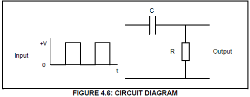
4.6.1 Identify the circuit diagram in FIGURE 4.6. (2)
4.6.2 Draw the output signal on the ANSWER SHEET for QUESTION 4.6.2 for the given circuit time constant. (3)
4.6.3 Explain how the output will be affected if the circuit time constant is increased. (2)
4.7 Refer to FIGURE 4.7 below and answer the questions that follow.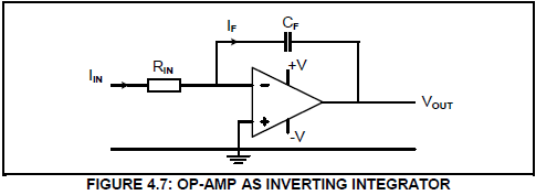
4.7.1 State the purpose of CF. (1)
4.7.2 Name THREE key operating points of the circuit in FIGURE 4.7. (3)
4.7.3 Draw the output signal on the ANSWER SHEET for QUESTION 4.7.3 if the signal below is applied to the input.
[60]
QUESTION 5: AMPLIFIERS
5.1 Compare Class A and Class B amplifiers with reference to the following:
5.1.1 Q-point (2)
5.1.2 Efficiency (2)
5.2 Refer to FIGURE 5.2 below and answer the questions that follow.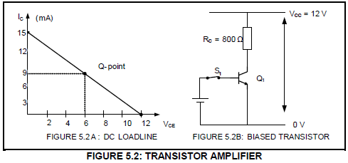
5.2.1 State ONE function of the collector resistor in FIGURE 5.2B. (1)
5.2.2 Explain how VCE becomes equivalent to VCC when S1 is open. (2)
5.3 With reference to biasing, explain Class C amplification. (2)
5.4 Refer to FIGURE 5.4 below and draw the output waveforms on the ANSWER SHEET for QUESTION 5.4 when the transistor is operating as the following: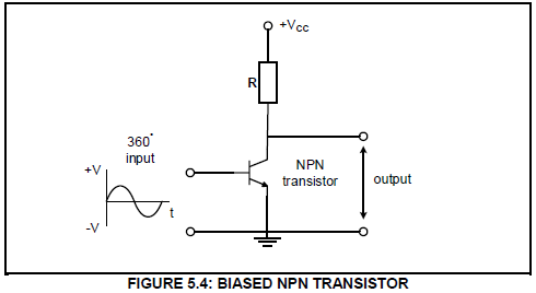
5.4.1 Class A amplifier (3)
5.4.2 Class AB amplifier (3)
5.5 State ONE undesirable condition that may occur due to the incorrect biasing of a transistor. (1)
5.6 Refer to FIGURE 5.6 below and answer the questions that follow.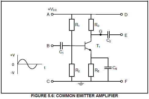
5.6.1 Explain why the circuit is called a common emitter amplifier. (2)
5.6.2 Name the points where the input signal and the load will be connected. (2)
5.6.3 Identify the TWO components that protect the transistor from thermal runaway. (2)
5.6.4 Draw the waveform that would appear between points G and F on the ANSWER SHEET for QUESTION 5.6.4. (3)
5.6.5 Draw the output waveform that would appear between points E and F on the ANSWER SHEET for QUESTION 5.6.5. (3)
5.7 Give TWO reasons for using coupling methods in amplifier circuits. (2)
5.8 A push-pull amplifier circuit has the following information:
Given:
Input power = 3 015 watts
Output power = 1 200 watts
Input voltage = 230 V
Output voltage = 219 V
Output current = 5,48 A
Output impedance = 40 Ω
Calculate the following:
5.8.1 Power gain in dB (3)
5.8.2 Voltage gain in dB (3)
5.9 Define the term gain of an amplifier. (2)
5.10 A certain cascaded amplifier (three-stage amplifier) arrangement has the following voltage gain:
AV1= 10, AV2= 15 and AV3= 20.
Calculate the total voltage gain. (3)
5.11 Refer to the amplifier circuit diagram in FIGURE 5.11 below and answer the questions that follow.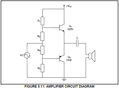
5.11.1 Identify the circuit diagram in FIGURE 5.11. (2)
5.11.2 Explain how cross-over distortion is eliminated in this amplifier. (2)
5.11.3 State the purpose of the resistors in the circuit diagram. (1)
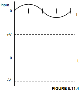
5.11.4 Draw a fully labelled output waveform of the circuit diagram on the ANSWER SHEET for QUESTION 5.11.4. (3)
5.12 FIGURE 5.12 below shows an FET oscillator circuit diagram. Answer the questions that follow.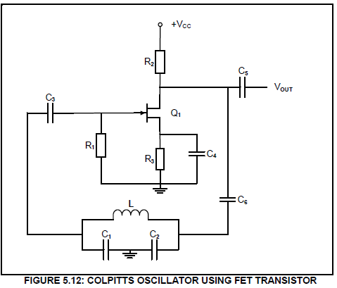
Compare the differences between RC and LC oscillators with reference to the following:
5.12.1 Feedback circuit (2)
5.12.2 Oscillation frequency (2)
5.13 Draw a modified tank circuit to change the Colpitts oscillator in FIGURE 5.12 into a Hartley oscillator. (3)
5.14 Name TWO functions of transistor Q1 in FIGURE 5.12. (2)
5.15 Name TWO similarities between an LC oscillator and an RC oscillator. (2)
[60]
TOTAL: 200
FORMULA SHEET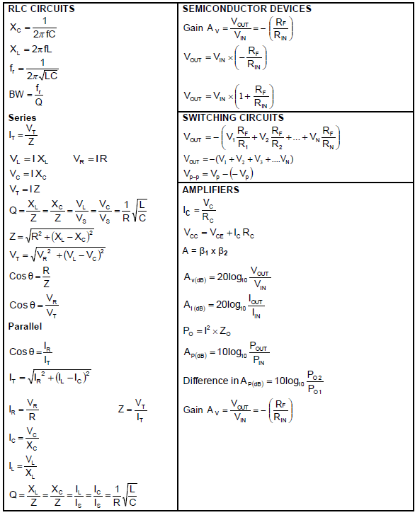
QUESTION 2: RLC CIRCUITS
2.3.4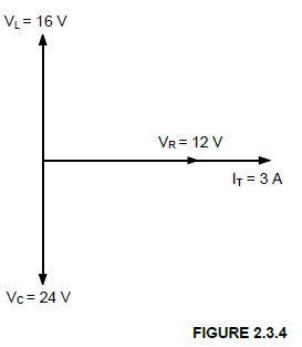
QUESTION 3: SEMICONDUCTOR DEVICES
3.4.3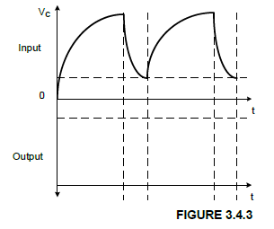
QUESTION 4: SWITCHING CIRCUITS
4.1.2
4.4.2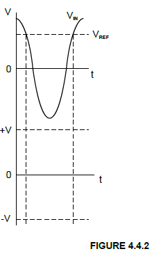
4.6.2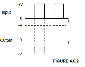
4.7.3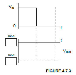
5.4.1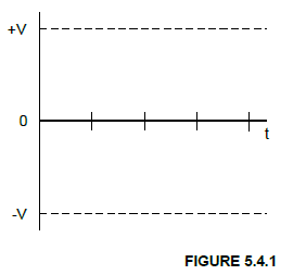
5.4.2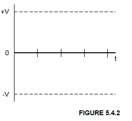
5.6.4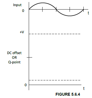
5.6.5
5.11.4