ELECTRICAL TECHNOLOGY(DIGITAL) GRADE 12 MEMORANDUM - NSC PAST PAPERS AND MEMOS NOVEMBER 2019
Share via Whatsapp Join our WhatsApp Group Join our Telegram GroupELECTRICAL TECHNOLOGY: DIGITAL
GRADE 12
NATIONAL SENIOR CERTIFICATE
MEMORANDUM
NOVEMBER 2019
INSTRUCTIONS TO THE MARKERS
- All questions with multiple answers imply that any relevant, acceptable answer should be considered.
- Calculations:
2.1 All calculations must show the formulae.
2.2 Substitution of values must be done correctly.
2.3 All answers MUST contain the correct unit to be considered.
2.4 Alternative methods must be considered, provided that the correct answer is obtained.
2.5Where an incorrect answer could be carried over to the next step, the first answer will be deemed incorrect. However, should the incorrect answer be carried over correctly, the marker has to re-calculate the values, using the incorrect answer from the first calculation. If correctly used, the candidate should receive the full marks for subsequent calculations.
2.6 Markers should consider when and where a candidate has rounded off in a calculation, as well as the subsequent effect it has on the final answer obtained. The calculation should therefore be awarded marks on merit. - These marking guidelines are only a guide with model answers. Alternative interpretations must be considered and marked on merit. However, this principle should be applied consistently throughout the marking session at ALL marking centres.
QUESTION 1: OCCUPATIONAL HEALTH AND SAFETY
1.1
- An employee with a sense of teamwork helps a team to meet its goals.
- Teamwork helps a team deliver quality work.
- Teamwork can win the respect of your co-workers.
- Working together as a team can improve discipline in the workshop.
- Teamwork will lead to improved productivity. (2)
1.2
1.2.1 The purpose of the Act is to:
- Provide for health and safety of persons at work.
- Protect against hazards arising from the activities of other people at work.
- Establish an advisory council for occupational health and safety and related matters.
- Provide for health and safety for persons in connection with the use of plant and machinery (2)
1.2.2 Workplace can be defined as any premises or place where a person performs work ü during the time of his employment. (2)
1.3
1.3.1 Employee. Learner, Supervisor, Team leader, Safety representative (1)
1.3.2 Health and safety representative. ü Inspector. (1)
1.4
- Remain calm.
- Stop whatever you are doing.
- Switch off machinery.
- Notify a responsible adult or teacher.
- If there is an emergency stop nearby activate it if necessary.
- Move in an orderly manner to the nearest assembly point.
NOTE: Procedure can be listed in any order (2)
[10]
QUESTION 2: SWITCHING CIRCUITS (GENERIC)
2.1
2.1.1
- – Bistable multivibrator
- – Monostable multivibrator (2)
2.1.2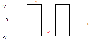
2 marks = 1 mark for each correct half cycle
If waveform is correctly drawn but inverted, 2 marks will be awarded
NOTE: Due to the +V instead of -V typo on the answer sheet, the following responses are also accepted. (2)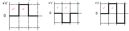
2.2
2.2.1 Resistors R1 and R2 are pull-up resistors.
Resistors R1 and R2 will hold both trigger pin 2 and reset pin 4 high. (2)
2.2.2 Trigger pin 2 will be pulled low and cause the IC output to 'flip' and rise high turning the LED on When set switch S1 is pressed, (3)
2.2.3 Threshold pin 6 is purposely held at 0 V causing the IC not to reset, keeping the output high when S1 is pressed. (3)
2.3
2.3.1 The output signal represents an inverting Schmitt trigger because the output signal is inverted with reference to the input signal.
OR
The output signal is at -VCC when triggered by the upper trigger voltage and swings to +VCC when triggered by the lower trigger voltage. (3)
2.3.2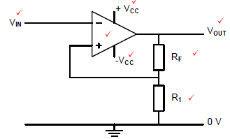
NOTE: Where a portion of the circuit is incorrect, the learner will lose those marks and will be awarded marks for the correct section / labels.
Any 7 correct labels (7)
2.4
2.4.1 Inverting comparator (2)
2.4.2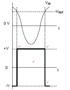
1 mark = inversion
1 mark = correct wave shape
2 marks = 1 mark for each correct trigger point. (4)
2.4.3 Change the connection of resistor R1 from the positive supply to the negative supply. (2)
2.5
2.5.1 The gain of the amplifier is determined by the ratio of the feedback resistance to the input resistance of each branch.
NOTE: Writing the formula only = 1 mark. (3)
2.5.2 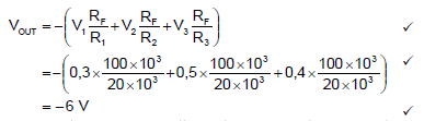 (3)
(3)
2.5.3 The amplifier is not saturated because the output voltage is less than the supply voltage. (2)
2.5.4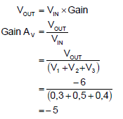 (3)
(3)
2.5.5 With a variable resistor in the feedback loop, the gain of the amplifier can be varied / controlled. (2)
2.5.6 If R2 is changed to 10 kΩ, the gain for V2 will increase causing the total output voltage to increase. (2)
2.6
2.6.1 RC passive differentiator
NOTE: RC circuit = 1mark (2)
2.6.2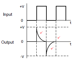
1 mark = positive pulse
1 mark = negative pulse
1 mark = correct orientation (3)
2.6.3 If the circuit time constant is increased, the capacitor will discharge slower producing a sagging square wave.
NOTE: If the learner draws the waveform and label correctly, mark on merit. (2)
2.7
2.7.1 CF provides a feedback connection from output to input. (1)
2.7.2 The inputs draw zero current.
The two inputs possess the same voltage at all times.
The capacitor will charge at a constant rate when a constant current is supplied.
NOTE: If the learner gives a correct account of the operation of the integrator as applied with the 741 op-amp, the answer must be marked on merit. (3)
2.7.3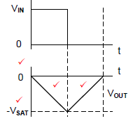
2 marks = correct labelling
2 marks = 1 mark for each correct half cycle
NOTE: The wave must be drawn correct before marks can be awarded for labelling. (4)
[60]
QUESTION 3: SEMICONDUCTOR DEVICES
3.1
3.1.1 Pin 1 is identified by being the first pin to the left and below the indentation. OR
Being closest to the dot in the body. (1)
3.1.2 Input stage or differential amplifier
Intermediate stage or high gain differential amplifier
Output stage or common collector (3)
3.1.3
- It stabilises the amplifier.
- Distortion of the output signal is reduced.
- The bandwidth increases. (2)
3.2
3.2.1 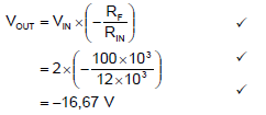 (3)
(3)
3.2.2 The amplifier is driven into saturation which causes the tops and bottoms to be clipped.
NOTE: If the learner identified that the input is fed into the inverting input, there will be a 180 degree phase shift on the output = 2 marks (2)
3.2.3 +15 volts –15 volts (2)
3.3
3.3.1 Dual in-line package (1)
3.3.2 Astable mode
Monostable mode
Bistable mode (3)
3.3.3 5 V (1)
3.4 When the trigger voltage rises above the threshold voltage, the output of a 555 timer will change state from high to low.
NOTE: If the answer is given as “Switch off” only = 1 mark (2)
[20]
QUESTION 4: DIGITAL AND SEQUENTIAL DEVICES
4.1 Polarisation (1)
4.2
4.2.1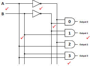
1 mark for inputs A,B
1 mark for inverters (NOT gates)
1 mark for outputs
1 mark for AND gates
1 mark each for connections
NOTE: Where a portion of the circuit is incorrect, he/she will lose those marks and will be awarded marks for the correct section / labels. (6)
OR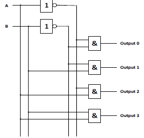
4.2.2
| Inputs | Outputs | ||||
| A | B | 0 | 1 | 2 | 3 |
| 0 | 0 | 1 | 0 | 0 | 0 |
| 0 | 1 | 0 | 1 | 0 | 0 |
| 1 | 0 | 0 | 0 | 1 | 0 |
| 1 | 1 | 0 | 0 | 0 | 1 |
(4)
TABLE 4.2.2
4.3
4.3.1 Clock (1)
4.3.2 The driver transistors are used to feed each LED in the display separately to ensure that all bars of a number are illuminated to the same level. (3)
4.3.3
| Inputs | Outputs | |||||||||
| A | B | C | D | a | b | c | d | e | f | g |
| 0 | 1 | 0 | 1 | 1 | 0 | 1 | 1 | 0 | 1 | 1 |
(4)
4.4
4.4.1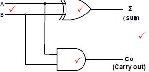
1 mark for inputs A,B
1 mark for outputs
1 mark for And gate
1 mark for XOR gate (4)
OR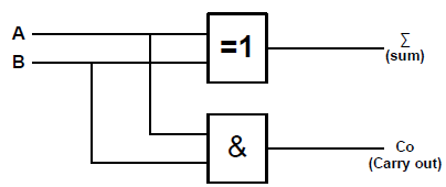
4.4.2
| INPUTS | OUTPUTS | ||
| A | B | Σ | Cº |
| 0 | 0 | 0 | 0 |
| 0 | 1 | 1 | 0 |
| 1 | 0 | 1 | 0 |
| 1 | 1 | 0 | 1 |
TABLE 4.4.2 (4)
4.5
4.5.1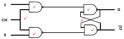
1 mark for input gate R
1 mark for output gate Q
1 mark for output gate ?
1 mark for latch
1 mark for clock connection
NOTE: Where a portion of the circuit is incorrect, the learner will lose those marks and will be awarded marks for the correct section / labels. (6)
OR
4.5.2
| INPUTS | OUTPUTS | |||
| CLK | S | R | Q | ? |
| | 0 | 0 | NO CHANGE | |
| | 0 | 1 | 0 | 1 |
| 1 | 0 | 1 | 0 | |
| | 1 | 1 | INDETERMINATE | |
INDETERMINATE (4)
4.6 Frequency divider
Decade counter
Binary coded decimal (BCD) counter (2)
4.7
- When a logic low '0' is applied to the circuit it has no effect on the JK flip-flop.
- When a logic high is applied to the inputs, the J and K inputs of each stage are held high '1'
- Turning them each into a single stage 'toggle' that will respond to the status of its preceding stage,
- After a clock pulse is only applied on the first flip flop it will change state.
- Going high '1' on the first pulse and low '0' on the next pulse.
- Rather than allow the counter to run through its full count term, a NAND gate is added with its two inputs connected to the outputs of the first and fourth flip-flop.
- Once the count reaches 1001 (decimal 9) the NAND gate's output will trigger low '0' thus activating the 'clear' inputs of each flip-flop,
- Re-setting them all to zero. ü and the process repeats itself.
NOTE: Although the following statement is wrong, if the learner writes it in the place of the second bullet, a mark must be awarded, because it is wrongly stated in the prescribed textbook - When a logic high '1' is applied to the circuit it immediately clears or resets the flip-flop back to its original position. (8)
4.8
4.8.1 Parallel-in; Serial-out shift register (1)
4.8.2 A = Clock,
B = 4-bit Parallel Data Input
B = Input, Parallel Data Input = 1 (2)
4.8.3 In the Parallel-in Serial-out shift register all four bits of the data are introduced to the register at the same time in parallel. (1)
4.8.4 It is shifted out, one bit at a time controlled by the clock input cycle. (1)
4.8.5 The circuit enables parallel data ü to be converted ü into serial format.
OR
The circuit enables parallel data, like an 8-bit word
- to be converted into serial format, or
- to mix a number of input lines together into a single stream of data
- that can be sent directly to a computer or be transmitted over a communication line. (3)
[55]
QUESTION 5: MICROCONTROLLERS
5.1 A microcontroller is a computer presented in a single integrated circuit which is dedicated to perform a task/s and execute one specific application.
OR
A microcontroller is an independent device, a computer on a chip that can perform a limited range of functions without needing to rely on other chips or devices.(3)
5.2
5.2.1 First, it fetches instructions and data from memory. It then decodesü the instructions which are written in binary code, then it executes the instruction before starting the cycle all over again.
OR
The operating cycle of a CPU follows a 'fetch-decode-execute’ cycle.
The operating cycle of a CPU follows a ‘Input-Process-Output’ cycle. (3)
5.2.2 The CIR holds the instruction ü that is currently being executed at a specific address.
OR
- The Current Instruction Register (CIR) splits the instruction into two parts.
- One part is decoded by the control unit ready for execution.
- The other part is the address of the data stored that needs to be used together with that instruction. (3)
5.2.3 The ADC detects a continuously variable (analogue) signal and changes this analogue signal, without altering its essential content, into a multi-level (digital) signal. (3)
5.2.4
- The timer is programmed to count to a predetermined number.
- Data is fed into the CIR via the MDB in parallel.
- The clock pulses together with the number being counted to determine the time duration.
- When the 8-bit count finally overflows the register, an output signal is generated on the following clock pulse.
- This could trigger an interrupt in the processor or set a bit that the processor can read.
- Once done the register is cleared on the next clock pulse.
OR
The timer accepts data, one bit at a time, controlled by the pulse rate of the clock, incrementing (adding one by one) for each pulse until the register overflows. (6)
5.3
- The RAM stores all the data that is required to be processed by the CPU during the execution of programmes.
OR - RAM can both read and write data into it.
- It can hold programmes, operating systems and data required by the system. (1)
5.4
5.4.1
- Simplex
- Duplex
- Half-duplex
- Full-duplex (2)
5.4.2
- Faster
- Higher Bandwidth (More bits can be transferred in a shorter time) (2)
5.4.3
- The system needs a clock signal to both transmitter and receiver.
- It operates on a primary/secondary configuration where one system (the transmitter) has control over the operation and the receiver is the secondary.
- The systems need to be synchronised. (2)
5.5
- Inter-integrated bus (I2C) is a powerful two wire bus
- That can support up to one thousand slave devices
- as well as supporting the communication of multiple masters
- Which, cannot talk to each other over the bus and have to take turns in using the bus lines.
- I2C uses start and stop sequences between masters and slaves over a two wire system.
- It works on a master-slave principle. (3)
5.6
5.6.1 Master (1)
5.6.2 Serial Clock Line (1)
5.6.3 Pull-up resistors, connected to a +5 V supply, are necessary for the lines (SCL and SDA) to go high. (2)
5.6.4 A slave cannot initiate a transfer over the I2C bus.
A slave interprets instructions received by the master. (1)
5.6.5
- I2C requires only two wires
- I2C supports multiple devices on the same bus without additional select lines
- I2C ensures that data sent is received by the slave device.
- I2C is cheaper to implement
- I2C supports multiple master devices
- I2C is less susceptible to noise than SPI (3)
5.7
5.7.1 Logic '1' between -3 V and -25 V
Logic '0' between +3 V and +25 V (2)
5.7.2 Used in low-data-rate short range applications such as;
- printers,
- modems,
- data projectors,
- CNC machine tools (3)
5.8
5.8.1 A program is a sequence of instructions that informs a computer how to perform a task. (2)
5.8.2 A flow diagram is a visual representation of steps and decisions ü needed to perform and complete a process. (2)
5.9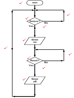
1 mark for Start symbol (1)
1 mark for Sensor symbol (1)
1 mark for Siren on symbol (1)
1 mark for Reset symbol (1)
1 mark for Siren off symbol (1)
1 mark for any one YES/NO statement (2)
1 mark each for THREE correct flow lines (3)
(10)
NOTE: Each design must be assessed on merit and variations should be allowed.
[55]
TOTAL: 200