ELECTRICAL TECHNOLOGY(DIGITAL) GRADE 12 QUESTIONS - NSC PAST PAPERS AND MEMOS NOVEMBER 2019
Share via Whatsapp Join our WhatsApp Group Join our Telegram GroupELECTRICAL TECHNOLOGY: DIGITAL
GRADE 12
NATIONAL SENIOR CERTIFICATE
NOVEMBER 2019
INSTRUCTIONS AND INFORMATION
- This question paper consists of FIVE questions.
- Answer ALL the questions.
- Answer the following questions on the attached ANSWER SHEETS:
QUESTIONS 2.1.2, 2.4.2, 2.6.2 and 2.7.3
QUESTIONS 4.2.2, 4.3.3, 4.4.2, 4.5.1 and 4.5.2 - Write your CENTRE NUMBER and EXAMINATION NUMBER on every ANSWER SHEET and hand them in with your ANSWER BOOK, whether you have used them or not.
- Sketches and diagrams must be large, neat and FULLY LABELLED.
- Show ALL calculations and round off answers correctly to TWO decimal places.
- Number the answers correctly according to the numbering system used in this question paper.
- You may use a non-programmable calculator.
- Calculations must include:
9.1 Formulae and manipulations where needed
9.2 Correct replacement of values
9.3 Correct answer and relevant units where applicable - A formula sheet is attached at the end of this question paper.
- Write neatly and legibly.
QUESTION 1: OCCUPATIONAL HEALTH AND SAFETY
1.1 Describe how teamwork improves work ethics. (2)
1.2 With reference to the Occupational Health and Safety Act, 1993 (Act 85 of 1993):
1.2.1 State TWO purposes of the Occupational Health and Safety Act, 1993 (Act 85 of 1993). (2)
1.2.2 Define the term workplace. (2)
1.3 An employer has a duty to report on occupational health and safety and related matters. Name ONE person they should inform when:
1.3.1 The allocated task is hazardous (1)
1.3.2 A major incident occurs (1)
1.4 State TWO general emergency procedures to be followed when the emergency siren is sounded at school. (2)
[10]
QUESTION 2: SWITCHING CIRCUITS
2.1 Refer to FIGURE 2.1 below and answer the questions that follow.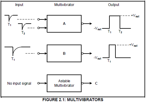
2.1.1 Identify multivibrators A and B. (2)
2.1.2 Draw the output signal of the astable multivibrator at C on the ANSWER SHEET for QUESTION 2.1.2. (2)
2.2 Refer to FIGURE 2.2 below and answer the questions that follow.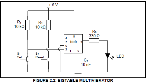
2.2.1 State the function of R1 and R2. (2)
2.2.2 Describe what happens when the set switch, S1, is pressed. (3)
2.2.3 Explain why threshold pin 6 is connected directly to ground. (3)
2.3 Refer to FIGURE 2.3 below and answer the questions that follow.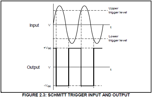
2.3.1 State whether the output signal represents an inverting or a non-inverting Schmitt trigger. Motivate your answer. (3)
2.3.2 Draw the circuit diagram of the Schmitt trigger consisting of two resistors and a 741 op-amp that will produce the output signal in FIGURE 2.3. (7)
2.4 Refer to FIGURE 2.4 below and answer the questions that follow.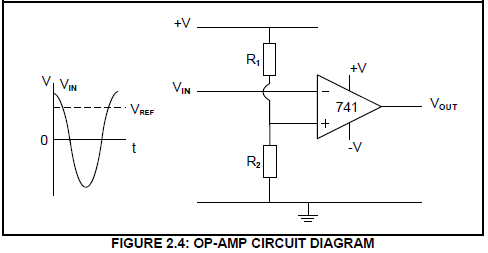
2.4.1 Identify the op-amp circuit diagram in FIGURE 2.4. (2)
2.4.2 Draw the output signal on the ANSWER SHEET for QUESTION 2.4.2. (4)
2.4.3 Explain how the reference voltage is made negative. (2)
2.5 Refer to FIGURE 2.5 below and answer the questions that follow.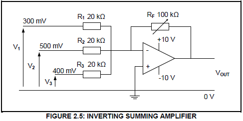
Given:
V1 = 300 mV
V2 = 500 mV
V3 = 400 mV
RF = 100 kΩ
R1 = R2 = R3 = 20 kΩ
2.5.1 Explain how the gain of this amplifier can be determined. (3)
2.5.2 Calculate the output voltage of the amplifier. (3)
2.5.3 Give a reason why the amplifier is NOT saturated. (2)
2.5.4 Calculate the gain of the amplifier using voltage values. (3)
2.5.5 Explain the advantage of using a variable resistor in the feedback loop instead of using a fixed resistor. (2)
2.5.6 Describe what will happen to the output voltage if the value of R2 is changed to 10 kΩ. (2)
2.6 Refer to FIGURE 2.6 below and answer the questions that follow.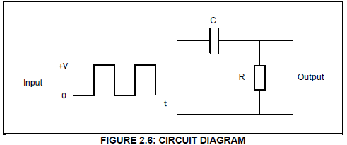
2.6.1 Identify the circuit diagram in FIGURE 2.6 (2)
2.6.2 Draw the output signal on the ANSWER SHEET for QUESTION 2.6.2 for the given circuit time constant. (3)
2.6.3 Explain how the output will be affected if the circuit time constant is increased. (2)
2.7 Refer to FIGURE 2.7 below and answer the questions that follow.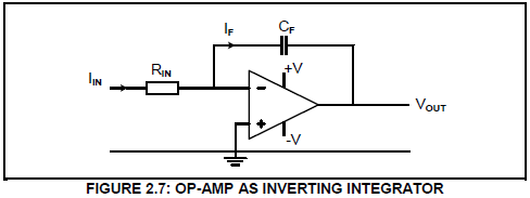
2.7.1 State the purpose of CF. (1)
2.7.2 Name THREE key operating points of the circuit in FIGURE 2.7. (3)
2.7.3 Draw the output signal on the ANSWER SHEET for QUESTION 2.7.3 if the signal below is applied to the input.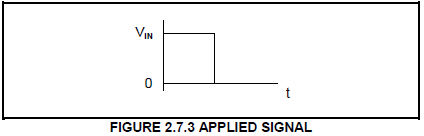
[60]
QUESTION 3: SEMICONDUCTOR DEVICES
3.1 Refer to FIGURE 3.1 below and answer the questions that follow.
3.1.1 State how you would identify pin 1 of the IC in FIGURE 3.1. (1)
3.1.2 List the THREE stages into which the internal circuit of the op-amp is divided. (3)
3.1.3 Give TWO reasons why negative feedback is important when the op-amp is used as a linear amplifier. (2)
3.2 FIGURE 3.2 below shows the op-amp as an inverting amplifier. Answer the questions that follow.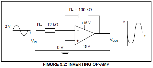
Given:
VIN = 2 V
RF = 100 kΩ
RIN = 12 kΩ
3.2.1 Calculate the output voltage based on the data given in the circuit. (3)
3.2.2 Explain why the output waveform is NOT an exact replica of the input waveform. (2)
3.2.3 Identify the maximum output voltages (Vout). (2)
3.3 Refer to the data sheet in FIGURE 3.3 below and answer the questions that follow.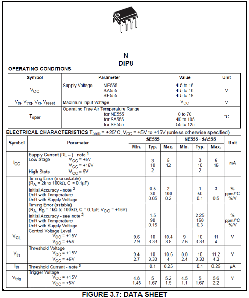
3.3.1 Rewrite the abbreviation DIP in full. (1)
3.3.2 Name THREE modes of operation of the NE555 IC. (3)
3.3.3 Identify the typical trigger voltage of the NE555 IC on the data sheet when the supply voltage is +15 V. (1)
3.4 Explain what will happen to the output of an NE555 IC when the trigger voltage rises above the threshold voltage level of 10 V. (2)
[20]
QUESTION 4: DIGITAL AND SEQUENTIAL DEVICES
4.1 State the light-altering principle of operation of the liquid crystal display (LCD). (1)
4.2 With reference to encoders and decoders, answer the questions that follow:
4.2.1 Draw the circuit diagram of a simple two-digit-binary-input-tofour-digit-decimal-output decoder using TWO NOT gates and FOUR AND gates. (6)
4.2.2 Complete the truth table of the two-digit-binary-input-tofour-digit-decimal-output decoder on the ANSWER SHEET forQUESTION 4.2.2.
| Inputs | Outputs | ||||
| A | B | 0 | 1 | 2 | 3 |
| 0 | 0 | ||||
| 0 | 1 | ||||
| 1 | 0 | ||||
| 1 | 1 | ||||
TABLE 4.2.2 (4)
4.3 FIGURE 4.3 below is the block diagram of a BCD-to-seven-segment decoder connected to a seven-segment LED display. Answer the questions that follow.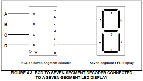
4.3.1 Label input W. (1)
4.3.2 Explain the function of the driver transistors found in the BCD-to seven-segment display decoder. (3)
4.3.3 Complete the truth table of a BCD to seven-segment decoder connected to a seven-segment LED display in TABLE 4.3.3 on the ANSWER SHEET for QUESTION 4.3.3.
| Inputs | Outputs | |||||||||
| A | B | C | D | a | b | c | d | e | f | g |
| 0 | 1 | 0 | 1 | 1 | 0 | 1 | ||||
TABLE 4.3.3 (4)
4.4 FIGURE 4.4 below represents the logic symbol of a HALF ADDER. Answer the questions that follow.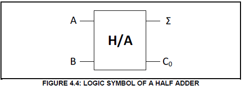
4.4.1 Draw the logic circuit of this half adder using an AND gate and an exclusive OR gate only. (4)
4.4.2 Complete the truth table of the half adder in TABLE 4.4.2 on the ANSWER SHEET for QUESTION 4.4.2.
| INPUTS | OUTPUTS | ||
| A | B | Σ | Co |
| 0 | 0 | 0 | |
| 0 | 1 | 0 | |
| 1 | 0 | 1 | |
| 1 | 1 | 1 | |
TABLE 4.4.2 (4)
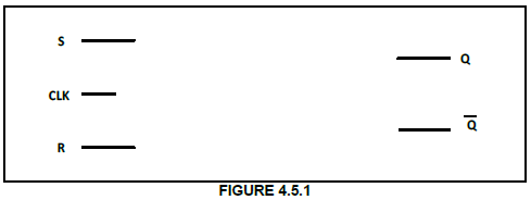
4.5 FIGURE 4.5 represents the logic symbol of a clocked RS-type flip flop.
Answer the questions that follow.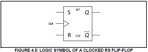
4.5.1 Draw the logic circuit of this flip flop on the ANSWER SHEET for QUESTION 4.5.1, using NAND gates only. (6)
4.5.2 Complete the truth table of this flip flop in TABLE 4.5.2 on the ANSWER SHEET for QUESTION 4.5.2.
| INPUTS | OUTPUTS | |||
| CLK | S | R | Q | Q ̅ |
| 0 | 0 | NO CHANGE | ||
| 0 | 1 | |||
| 1 | 0 | |||
| 1 | 1 | INDETERMINATE | ||
TABLE 4.5.2 (4)
4.6 Name TWO applications of counters. (2)
4.7 FIGURE 4.7 below represents a four-stage asynchronous binary-to-BCD counter using JK flip-flops. Explain the operation of this counter.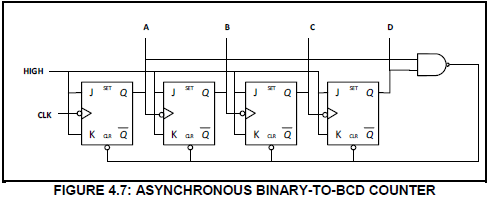
4.8 Refer to FIGURE 4.8 below and answer the questions that follow.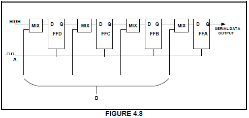
4.8.1 Identify the shift register in FIGURE 4.8. (1)
4.8.2 Label A and B. (2)
4.8.3 Describe how data is introduced to the register. (1)
4.8.4 Describe how data is shifted out of the register. (1)
4.8.5 State THREE uses of this register. (3)
[55]
QUESTION 5: MICROCONTROLLERS
5.1 Define the term microcontroller. (3)
5.2 With reference to the hardware of microcontrollers:
5.2.1 Describe the operating cycle of a CPU. (3)
5.2.2 Explain the function of the current instruction register (CIR). (3)
5.2.3 State the purpose of an analogue-to digital-converter (ADC). (3)
5.2.4 FIGURE 5.2.4 below is the block diagram of a simple counter/timer. Explain the operation of this timer.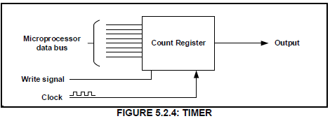
5.3 State the function of the random access memory (RAM) with reference to the CPU of a microcontroller. (1)
5.4 With reference to communication in a microcontroller:
5.4.1 Name TWO methods of sending data (2)
5.4.2 State the advantages of parallel communication (2)
5.4.3 Name the disadvantages of synchronous communication (2)
5.5 Describe the inter-integrated bus (I2C) as a type of communication peripheral. (3)
5.6 FIGURE 5.6 is the block diagram of the I2C bus system. Answer the questions that follow.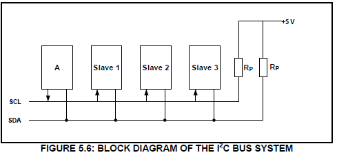
5.6.1 Label block A. (1)
5.6.2 What does the abbreviation SCL stand for? (1)
5.6.3 Explain the function of the pull-up resistors. (2)
5.6.4 Name ONE characteristic of the slave. (1)
5.6.5 List THREE advantages of the I2C bus. (3)
5.7 With reference to the RS-232 communication protocol, answer the following questions:
5.7.1 State the operating voltages for logic '1' and logic '0'. (2)
5.7.2 List THREE applications of the RS-232. (3)
5.8 With reference to microcontrollers:
5.8.1 Define the term program. (2)
5.8.2 Define the term flow diagram. (2)
5.9 Design a flow diagram of an alarm system for a storage room which has ONE sensor that must monitor the access door to the room. The alarm must sound if the sensor is activated. The system must include a reset function. NO time delay is needed. (10)
[55]
TOTAL: 200
FORMULA SHEET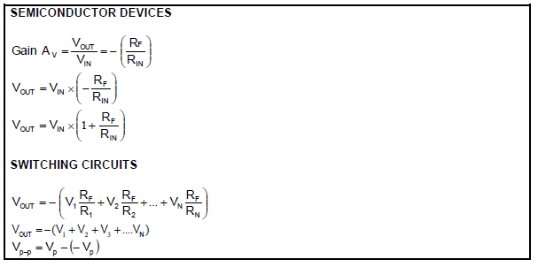
QUESTION 2: SWITCHING CIRCUITS
2.1.2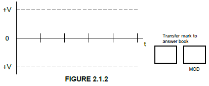
2.4.2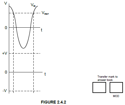
2.6.2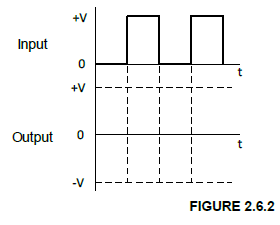
2.7.3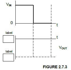
4.5.1