ELECTRICAL TECHNOLOGY:DIGITAL GRADE 12 QUESTIONS - NSC PAST PAPERS AND MEMOS MAY/JUNE 2019
Share via Whatsapp Join our WhatsApp Group Join our Telegram GroupELECTRICAL TECHNOLOGY:DIGITAL
GRADE 12
NATIONAL SENIOR CERTIFICATE EXAMINATIONS
MAY/JUNE 2019
INSTRUCTIONS AND INFORMATION
- This question paper consists of FIVE questions.
- Answer ALL the questions.
- Answer the following questions on the attached ANSWER SHEETS:
QUESTIONS 2.2.1, 2.4.2, 2.4.4, 2.5.2, 2.6.3 and 2.8.2
QUESTIONS 4.3.1, 4.3.2, 4.4, 4.5 and 4.7 - Write your CENTRE NUMBER and EXAMINATION NUMBER on every ANSWER SHEET and hand them in with your ANSWER BOOK, whether you have used them or not.
- Sketches and diagrams must be large, neat and fully labelled.
- Show ALL calculations and round off answers correctly to TWO decimal places.
- Number the answers correctly according to the numbering system used in this question paper.
- You may use a non-programmable calculator.
- Show the units for ALL answers and calculations.
- A formula sheet is attached at the end of this question paper.
- Write neatly and legibly.
QUESTION 1: OCCUPATIONAL HEALTH AND SAFETY (GENERIC)
1.1 Define the term accident with reference to the Occupational Health and Safety Act, 1993 (Act 85 of 1993). (3)
1.2 State TWO procedures to follow when evacuating a workshop in an emergency. (2)
1.3 Explain why you must protect yourself when helping a person who is being shocked by electricity. (1)
1.4 Briefly describe a third degree burn. (2)
1.5 Explain why a person should not interfere with, or misuse, equipment in the workshop that is provided for health or safety. (2)
[10]
QUESTION 2: SWITCHING CIRCUITS (GENERIC)
2.1 Explain the term bistable with reference to multivibrators. (1)
2.2 Refer to FIGURE 2.2 below and answer the questions that follow.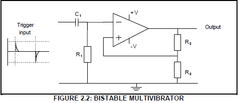
2.2.1 Draw the output signal with reference to the trigger input on ANSWER SHEET 2.2.1. (2)
2.2.2 Explain what happens in the circuit at switch-on until a trigger pulse is received. (3)
2.3 FIGURE 2.3 below shows the typical waveforms of a 741 op amp connected as a monostable multivibrator. Answer the questions that follow.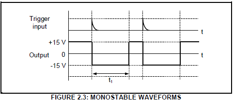
2.3.1 Explain what happens to the output with reference to t1 when a trigger input is received. (3)
2.3.2 State how the time period t1 can be varied. (2)
2.3.3 Explain the extent of the voltage swing at the output when a trigger pulse is received. (3)
2.4 Refer to FIGURE 2.4 below and answer the questions that follow.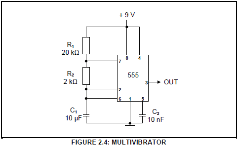
2.4.1 Identify the multivibrator in FIGURE 2.4 above. (1)
2.4.2 Draw the charging and discharging waveform of capacitor C1 on ANSWER SHEET 2.4.2. (3)
2.4.3 Explain why there is a difference in the charging and discharging times of the capacitor. (2)
2.4.4 Draw the output signal at pin 3 on ANSWER SHEET 2.4.4. (2)
2.5 Refer to FIGURE 2.5 below and answer the questions that follow.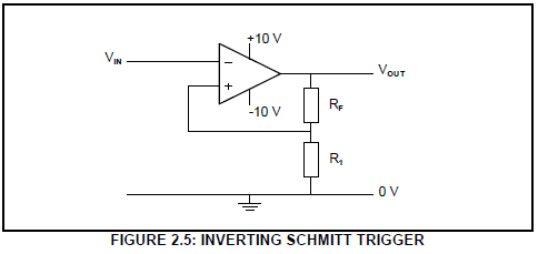
2.5.1 Explain the function of resistors RF and R1. (3)
2.5.2 Draw the output signal on ANSWER SHEET 2.5.2 if the signal in FIGURE 2.5.2 below is applied to the input of the Schmitt trigger.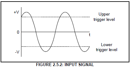
2.5.3 Describe how an increase in the value of RF will affect the trigger voltage. (3)
2.6 Refer to FIGURE 2.6 below and answer the questions that follow.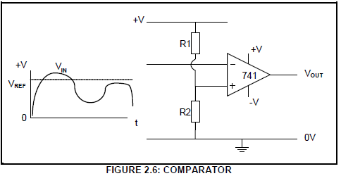
2.6.1 Explain what is meant by open loop with reference to FIGURE 2.6. (2)
2.6.2 Describe the principles of operation of a comparator. (6)
2.6.3 Draw the output signal on ANSWER SHEET 2.6.3. (2)
2.7 Refer to FIGURE 2.7 below and answer the questions that follow.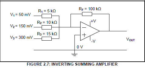
2.7.1 State how an additional input signal can be added to the summing amplifier. (1)
2.7.2 Calculate the output voltage for the inverting summing amplifier above. (3)
2.7.3 State why the answer to QUESTION 2.7.2 is negative. (1)
2.8 Refer to FIGURE 2.8 below and answer the questions that follow.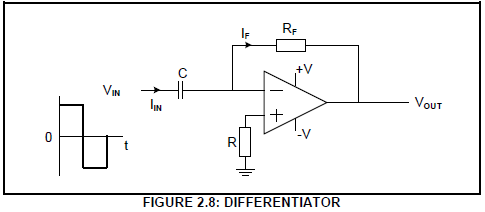
2.8.1 Give THREE reasons why it is advisable to connect an op amp to a passive RC differentiator. (3)
2.8.2 Draw the output signal on ANSWER SHEET 2.8.2. (2)
2.9 Give ONE reason for using a passive RC integrator circuit. (1)
2.10 FIGURE 2.10 below shows the output waveform of a passive RC-integrator displayed on the screen of an oscilloscope. Refer to the figure below and answer the questions that follow.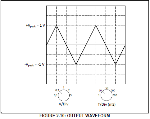
2.10.1 Identify the voltage per division setting. (1)
2.10.2 Determine the peak-to-peak voltage (3)
2.10.3 Determine how many complete cycles are displayed. (1)
2.10.4 Explain how a short RC time constant will affect the output of a passive RC integrator.
(3)
[60]
QUESTION 3: SEMICONDUCTOR DEVICES (SPECIFIC)
3.1 FIGURE 3.1 below shows two signals with the same frequency and amplitude that are applied onto the inputs of a 741 op amp. Answer the questions that follow.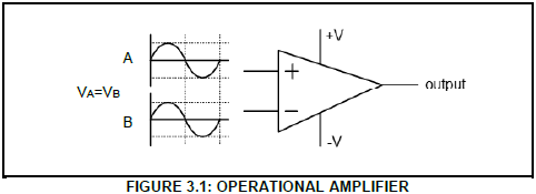
3.1.1 Write down the typical operating (supply) voltages of an op amp. (1)
3.1.2 Determine the value of the output voltage. (1)
3.1.3 Describe what will happen to the output signal if the amplitude of the signal on the non-inverting input is increased. (3)
3.2 Refer to FIGURE 3.2 below and answer the questions that follow.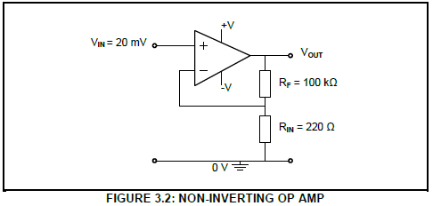
3.2.1 Identify the type of feedback in the circuit. (1)
3.2.2 Calculate the output voltage of the amplifier. (3)
3.3 FIGURE 3.3 below shows the internal block diagram of the 555 IC. Answer the questions that follow.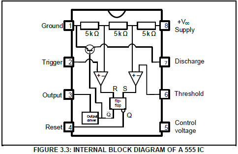
3.3.1 Name the THREE primary building blocks of the 555 IC. (3)
3.3.2 Explain the function of the three 5 kΩ resistors. (2)
3.4 Refer to FIGURE 3.4 below and answer the questions that follow.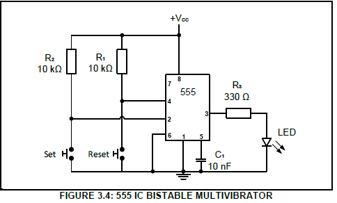
3.4.1 State the typical operating voltages for a 555 IC. (1)
3.4.2 Name TWO modes of operation of a 555, besides the bistable mode. (2)
3.4.3 Explain the operation of the 555 when connected in the bistable mode. (3)
[20]
QUESTION 4: DIGITAL AND SEQUENTIAL DEVICES (SPECIFIC)
4.1 Explain the term polarisation as used in the operation of a liquid crystal display (LCD.) (3)
4.2 Refer to the LED seven-segment display and explain the difference between a common anode and a common cathode. (4)
4.3 Refer to FIGURE 4.3 below and determine the binary code at the output when the following input switches are pressed. Write the answers on ANSWER 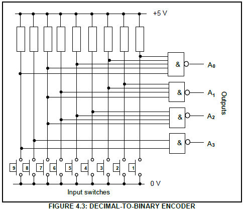
4.3.1 Switch 1 (4)
4.3.2 Switch 5 (4)
4.3.3 Briefly describe the STATE of the input switches if all outputs are ZERO. (2)
4.4 Study FIGURE 4.4 below of the logic circuit of a full adder using two halfadders and an OR-gate. Use the table on ANSWER SHEET 4.4 to complete the truth table.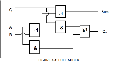
4.5 FIGURE 4.5 below represents the logic symbol of a clocked D-type flip-flop.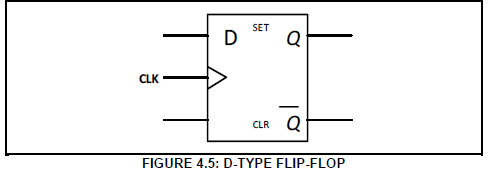
4.5.1 Draw the logic circuit of this flip-flop using NAND gates, NOR gates and an inverter. (6)
4.5.2 Complete the truth table of this flip-flop in TABLE 4.5.2 below on ANSWER SHEET 4.5.2.
| INPUTS | OUTPUTS | |||
| CLK | CLK | D | Q | Q |
| 0 | 0 | Latch | Latch | |
| 0 | 1 | Latch | Latch | |
| 1 | 0 | 0 | 1 | |
| 1 | 1 | 1 | 0 | |
TABLE 4.5.2 (4)
4.6 State TWO applications of the up/down counter. (2)
4.7 FIGURE 4.7 below shows a three-stage asynchronous ripple counter.
Complete the timing diagram on ANSWER SHEET 4.7.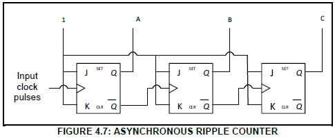
4.8 Explain why the circuit in FIGURE 4.7 is called asynchronous. (3)
4.9 State how many clock pulses the following shift registers need to shift a 4-bit input from the input to the output. Each shift register consists of four D-type flip-flops.
4.9.1 Serial in-serial out shift register (SISU) (1)
4.9.2 Serial in-parallel out shift register (SIPO) (1)
4.9.3 Parallel in-parallel out shift register (PIPO) (1)
4.10 Explain how a parallel in-serial out shift register (PISO) consisting of four D-type flip-flops will shift a 4-bit input to the output. (4)
[55]
QUESTION 5: MICROCONTROLLERS (SPECIFIC)
5.1 State TWO uses of a microcontroller in industrial control devices. (2)
5.2 State the basic function that random access memory (RAM) performs. (2)
5.3 State the basic function of a read-only memory (ROM). (2)
5.4 Refer to communication in a microcontroller and answer the questions that follow.
5.4.1 Draw the block diagram of a microcontroller, clearly indicating the THREE system buses. (9)
5.4.2 Define the term interface. (2)
5.5 Refer to registers within the CPU and answer the questions that follow.
5.5.1 Explain the function of a programme counter. (3)
5.5.2 Explain the function of a memory address register. (2)
5.6 State ONE type of communication protocol. (1)
5.7 Define communication protocol. (2)
5.8 Illustrate the following data transfer methods with a block diagram:
5.8.1 Serial (4)
5.8.2 Parallel (4)
5.9 Refer to a serial communication interface and answer the questions that follow.
5.9.1 Write out the acronym UART in full. (1)
5.9.2 Explain the function of the UART. (4)
5.10 Refer to software of microcontrollers.
5.10.1 Explain the term flowchart. (2)
5.10.2 Define an algorithm. (2)
5.10.3 Describe an instruction cycle. (3)
5.11 Study the following algorithm and draw a flow chart thereof:
- A bistable device has two stable states.
- It is set by an input going high, where it stays until it is reset by a second input.
- After resetting, the output returns to the low state.
- The device has a single output. (10)
[55]
TOTAL: 200
FORMULA SHEET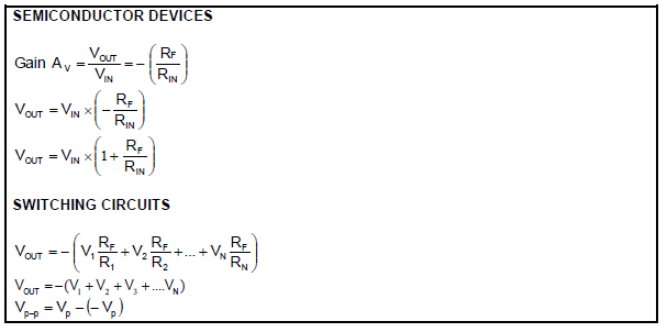
ANSWER SHEET 2.2.1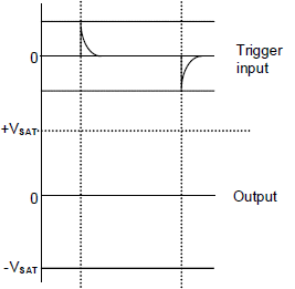
ANSWER SHEET 2.4.2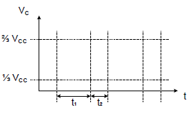
ANSWER SHEET 2.4.4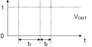
ANSWER SHEET 2.5.2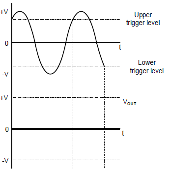
ANSWER SHEET 2.6.3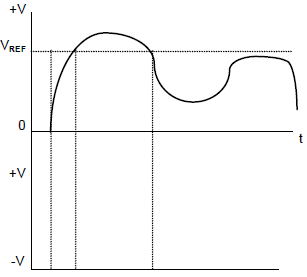
ANSWER SHEET 2.8.2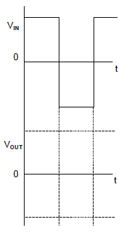
ANSWER SHEET 4.3.1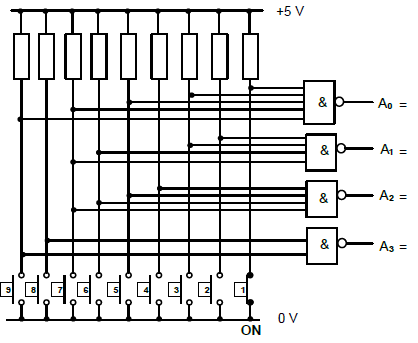
ANSWER SHEET 4.3.2
ANSWER SHEET 4.4
| INPUTS | OUTPUTS | |||
| Ci | A | B | Sum | Co |
| 0 | 0 | 0 | 0 | |
| 0 | 0 | 1 | 0 | |
| 0 | 1 | 0 | 1 | |
| 0 | 1 | 1 | 1 | |
| 1 | 0 | 0 | 0 | |
| 1 | 0 | 1 | 1 | |
| 1 | 1 | 0 | 0 | |
| 1 | 1 | 1 | 1 | |
ANSWER SHEET 4.5.2
| INPUTS | OUTPUTS | |||
| CLK | CLK | D | Q | Q |
| 0 | 0 | Latch | ||
| 0 | 1 | Latch | ||
| 1 | 0 | 0 | ||
| 1 | 1 | 1 | ||
ANSWER SHEET 4.7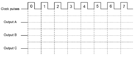
(8)