ELECTRICAL TECHNOLOGY:DIGITAL GRADE 12 MEMORANDUM - NSC PAST PAPERS AND MEMOS MAY/JUNE 2019
Share via Whatsapp Join our WhatsApp Group Join our Telegram GroupELECTRICAL TECHNOLOGY:DIGITAL
GRADE 12
NATIONAL SENIOR CERTIFICATE EXAMINATIONS
MEMORANDUM
MAY/JUNE 2019
INSTRUCTIONS TO THE MARKERS
- All questions with multiple answers imply that any relevant, acceptable answer should be considered.
- Calculations:
2.1 All calculations must show the formulae.
2.2 Substitution of values must be done correctly.
2.3 All answers MUST contain the correct unit to be considered.
2.4 Alternative methods must be considered, provided that the correct answer is obtained.
2.5 Where an incorrect answer could be carried over to the next step, the first answer will be deemed incorrect. However, should the incorrect answer be carried over correctly, the marker has to re-calculate the values, using the incorrect answer from the first calculation. If correctly used, the candidate should receive the full marks for subsequent calculations.
2.6 Markers should consider that learner answers may deviate slightly from the guideline, depending on how and where in the calculation rounding off was used. - This marking guideline is only a guide with model answers. Alternative interpretations must be considered and marked on merit. However, this principle should be applied consistently throughout the marking session at ALL marking centres.
QUESTION 1: OCCUPATIONAL HEALTH AND SAFETY (GENERIC)
1.1 An accident is an unplanned, uncontrolled event ✓ caused by unsafe acts and or unsafe conditions ✓ resulting in a personal injury, illness or the death of an employee. ✓
An accident means an accident arising out of and in the course of an employee’s employment and resulting in personal injury, illness or the death of the employee.
Note: The definition in the textbook is flawed but will be accepted. (3)
1.2 Move in an orderly manner. ✓
Follow the evacuation route as displayed in your workshop. ✓
Move to the designated assembly point in a calm and orderly manner. (2)
1.3 To prevent oneself form being shocked, ✓ therefore precautions must be taken to isolate oneself when rendering assistance.
To prevent injury. (1)
1.4 A third degree burn occurs when all layers of skin have been burnt, ✓ causing permanent skin damage affecting fat, muscle and even bone. ✓
A serious burn deserves 1 mark (2)
1.5 A person who intentionally and recklessly interferes with equipment will cause damages ✓ and this will render equipment unsafe and compromise the safety of the user. ✓ (2)
[10]
QUESTION 2: SWITCHING CIRCUITS (GENERIC)
2.1 Bistable refers to two stable states, either high or low in multivibrators (1)
2.2
2.2.1 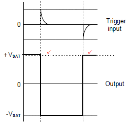
NOTE R1 acts as a pull down resistor ensuring that during switch on, the output will start at +VSAT
If the output is drawn inverted, 1 mark will be awarded for identifying both correct trigger points. (2)
2.2.2
- At switch-on, the voltage on the inverting input is zero ü while a small voltage from the voltage divider appears at the non-inverting terminal.
- This immediately drives the Op-amp into a state of positive saturation
- Where it will remain until a trigger pulse is received.
R1 acts as a pull down resistor ensuring that during switch on, the output will start at +VSAT (3)
2.3
2.3.1
- When a trigger input is received the output will change from positive saturation to negative saturation
- It will remain in this state for a pre-determined time (t1).
- and then return back to the original state.
If the learner mentions a square wave, 1 mark is awarded (3)
2.3.2 The switched time can be varied by changing the value of either the resistor ü or capacitor in the charging RC-circuit. (2)
2.3.3
- In the resting condition the output is driven to positive saturation (+15 V).
- When a trigger pulse is received, the output of the switching current will switch to negative saturation (-15 V).
- Therefore the change in voltage from positive saturation to negative saturation adds up to a total change of 30 V. (3)
2.4
2.4.1 Astable multivibrator (1)
2.4.2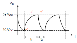 (3)
(3)
2.4.3 The capacitor charges through (R1+R2), causing a long RC time constant, but discharges through only R2 causing a short time constant. (2)
2.4
2.4.4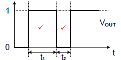
NOTE: If the output is inverted, 1 mark will be awarded for identifying both trigger points correctly. (2)
2.5
2.5.1
- RF and R1 creates a voltage divider.
- It divides the output voltage resulting in a portion of the output voltage appearing across R1.
- A fraction of the voltage across R1 is fed back to the Op-amp's non-inverting input. (3)
2.5.2 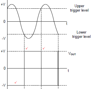
NOTE:
1 mark = correct orientation
2 marks = 1 mark for each correctly identified trigger point. (3)
2.5.3
- If the value of RF increases, the voltage across R1 will decrease according to Kirchhoff's voltage law.
- Therefore the voltage fed back to the non-inverting input will decrease.
- This will lead to a decrease in trigger voltage. (3)
2.6
2.6.1 Open loop is when there is no feedback resistor between the output and input of the circuit. (2)
2.6.2
- Voltage divider resistors R1 and R2 set up the reference voltage VREF
- The reference voltage is fed back to the non-inverting input of the Op-amp.
- The comparator compares the input voltage VIN to the reference voltage VREF.
- The gain of the Op-amp is ±100 000 because of the open loop connection.
- Whenever there is a fraction of a millivolt difference between VIN and VREF, this difference will be amplified.
- The Op-amp will be driven into either one of the saturation states ü (6)
2.6.3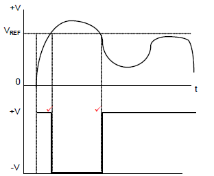
NOTE:
1 mark = correct orientation
1 mark = identifying both trigger points. (2)
2.7
2.7.1 By adding another input resistor to the summing amplifier input.(1)
2.7.2 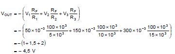 (3)
(3)
2.7.3 The answer in 2.7.2 is negative because the inputs are fed into the inverting input, which will cause the output to be 180° out of phase. (1)
2.8
2.8.1 It improves input and output impedances
It improves output gain
It improves the stability of the circuit (3)
2.8.2
This waveform is incorrectly given in the textbook, but must be accepted.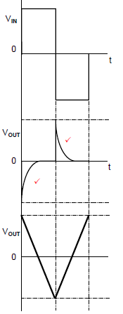
This is the correct output waveform of the Op-amp differentiator. (2)
2.9 A passive RC integrator is widely used in electronics to convert square waves into triangular waves.(1)
2.10
2.10.1 0,5 V per division. (1)
2.10.2 Vp-p = Vp -(-Vp) Vp-p = NO.div x V per div
= 1-(-1) = 4 x 0.5V
=2V = 2V
If only 2 V is metioned
3 marks (3)
2.10.3 Two complete cycles (1)
2.10.4
- A short RC time constant will cause the capacitor to charge and discharge completely.
- This will resemble a square wave output signal with rounded leading and trailing edges. (3)
[60]
QUESTION 3: SEMICONDUCTOR DEVICES (SPECIFIC)
3.1
3.1.1 +5 V/-5 V to +15 V/-15 V (1)
3.1.2 0 V (common mode rejection) (1)
3.1.3
- If the amplitude of the signal on the non-inverting input is increased, the Op-amp will amplify the difference between the two inputs.
- Because the non-inverting input is bigger than the inverting input,
- The output signal will now be in phase with the non-inverting input (3)
3.2
3.2.1 Negative feedback (1)
3.2.2
3.3
3.3.1 Two comparators / amplifiers
One R/S flip-flop
Three 5 kΩ resistors /voltage divider network
Transistor/Output driver (3)
3.3.2
- The three 5 kΩ resistors divide the supply voltage ü into two stepped down voltages of 1/3 and 2/3 of the supply voltage. (2)
3.4
3.4.1 +5 V to +18 V
3.4.2 Astable
Monostable
Schmitt trigger
3.4.3
- In the bistable mode the 555 works as a flip-flop with two stable states.
- When a trigger pulse is applied to pin 2, the circuit changes state to high '1' or set and remains in that state.
- When a trigger pulse is applied to pin 4, the circuit then changes state to low '0' or reset and remains in that state. (3)
[20]
QUESTION 4: DIGITAL AND SEQUENTIAL DEVICES (SPECIFIC)
4.1
- Polarisation is the application of a polarising filter as a grid that allows light of a single orientation to pass.
- In a LCD display two layers of polarized glass can be aligned or misaligned electrically to pass or block light. (3)
4.2
- In a COMMON ANODE the anodes of all eight LED's are connected together to a common positive voltage rail.
- In a COMMON CATHODE all eight LED cathodes are internally connected to a common 0 V ground. (4)
4.3
4.3.1 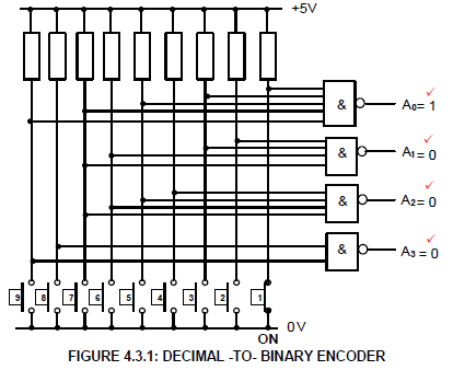 (4)
(4)
4.3.2 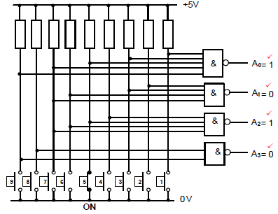 (4)
(4)
4.3.3 The outputs of figure 4.3 will be ZERO if all input switches are switched OFF. (2)
4.4
| INPUTS | OUTPUTS | |||
| Ci | A | B | Sum | Co |
| 0 | 0 | 0 | 0 | 0 |
| 0 | 0 | 1 | 1 | 0 |
| 0 | 1 | 0 | 1 | 0 |
| 0 | 1 | 1 | 0 | 1 |
| 1 | 0 | 0 | 1 | 0 |
| 1 | 0 | 1 | 0 | 1 |
| 1 | 1 | 0 | 0 | 1 |
| 1 | 1 | 1 | 1 | 1 |
FIGURE 4.4: FULL ADDER TRUTH TABLE (8)
4.5
4.5.1 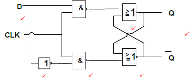 (6)
(6)
4.5.2
| INPUTS | OUTPUTS | |||
| CLK | CLK | D | Q | Q |
| | 0 | 0 | Latch | Latch |
| | 0 | 1 | Latch | Latch |
| | 1 | 0 | 0 | 1 |
| | 1 | 1 | 1 | 0 |
TABLE 4.5.2 (4)
4.6
- Robotics
- Computer Numeric Control (CNC) machines. (2)
4.7 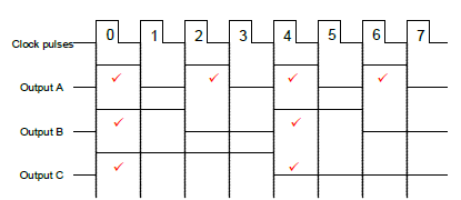 (8)
(8)
4.8 The circuit in FIGURE 4.7 is called ASYNCHRONOUS because the JK flip flops are not triggered at the same time causing their outputs not to change states at the same time. (3)
4.9
4.9.1 8 clock pulses. (1)
4.9.2 4 clock pulses. (1)
4.9.3 1 clock pulse. (1)
4.10 All four bits of the input will simultaneously ü be loaded to the input of all the flip-flops. After one clock pulse each flip-flop will shift its input to its output. This process will repeat itself for four clock pulses ü so that the complete 4-bit input is available at the output.(4)
[55]
QUESTION 5: MICROCONTROLLERS (SPECIFIC)
5.1 Microcontrollers are used in Industrial control devices:
- Industrial instrumentation
- Monitoring
- Process control
- Cooling systems (2)
5.2 The RAM stores all the data that is required to be processed by the CPU during the execution of programmes. (2)
5.3 The ROM contains information that is permanently required. It holds the programmes, operating systems and data required by the system to be booted up when it is turned on. (2)
5.4
5.4.1 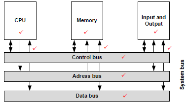 (9)
(9)
5.4.2 A shared boundary across which two separate components of a computer system exchanges information.(2)
5.5
5.5.1 It counts the number of instructions that have been executed, adding one each time. (3)
5.5.2 The MAR stores the address of the next instruction to be executed by the processor. (2)
5.6 RS 232 or RS 485 (1)
5.7 Communication protocol is a set of rules that allow two electronic devices to connect and exchange data. (2)
5.8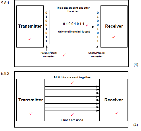
5.9
5.9.1 UART is a Universal Asynchronous Receiver Transmitter (1)
5.9.2 This communication peripheral sends and receives data serially.It converts parallel data to a serial data string and vice versa through the RX/TX line. (4)
5.10
5.10.1 A flowchart is a pictorial version of an algorithm and illustrates the flow of a program. (2)
5.10.2 An algorithm is a precise set of procedures to be followed in order to solve a problem. (2)
5.10.3 In the cycle, the CPU fetches a program instruction from its memory, decodes the instruction, considers all inputs and then executes that instruction.(3)
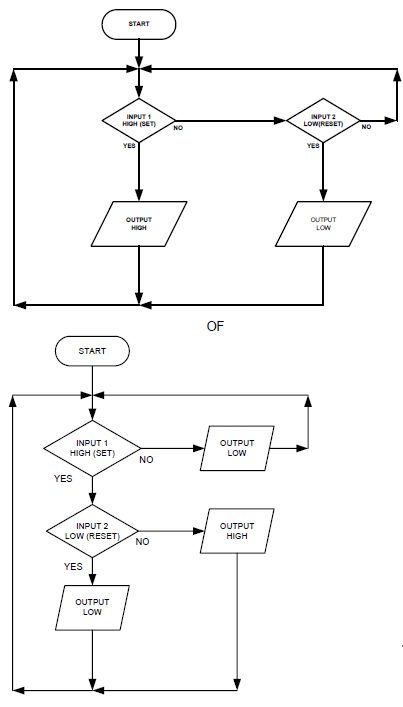
5.11 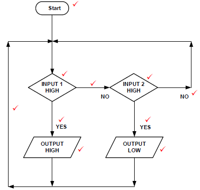 (10)
(10)
[55]
TOTAL: 200