ELECTRICAL TECHNOLOGY:ELECTRONICS GRADE 12 QUESTIONS - NSC PAST PAPERS AND MEMOS MAY/JUNE 2019
Share via Whatsapp Join our WhatsApp Group Join our Telegram GroupELECTRICAL TECHNOLOGY: ELECTRONICS
GRADE 12
NATIONAL SENIOR CERTIFICATE EXAMINATIONS
MAY/JUNE 2019
INSTRUCTIONS AND INFORMATION
- This question paper consists of SIX questions.
- Answer ALL the questions.
- Sketches and diagrams must be large, neat and fully labelled.
- Show ALL calculations and round off answers correctly to TWO decimal places.
- Number the answers correctly according to the numbering system used in this question paper.
- You may use a non-programmable calculator.
- Show the units for ALL answers of calculations.
- A formula sheet is attached at the end of this question paper.
- Write neatly and legibly.
QUESTION 1: OCCUPATIONAL HEALTH AND SAFETY (GENERIC)
1.1 Define the term accident with reference to the Occupational Health and Safety Act, 1993 (Act 85 of 1993). (3)
1.2 State TWO procedures to follow when evacuating a workshop in an emergency. (2)
1.3 Explain why you must protect yourself when helping a person who is being shocked by electricity. (1)
1.4 Briefly describe a third degree burn. (2)
1.5 Explain why a person should not interfere with, or misuse, equipment in the workshop that is provided for health or safety. (2)
[10]
QUESTION 2: RLC CIRCUITS (GENERIC)
2.1 Define the following terms:
2.1.1 Capacitive reactance (2)
2.1.2 Inductive reactance (2)
2.2 FIGURE 2.2 below represents an RLC series circuit that consists of a 25 Ω resistor, a 44 mH inductor and a 120 μF capacitor, all connected across a 120 V/60 Hz supply. Answer the questions that follow.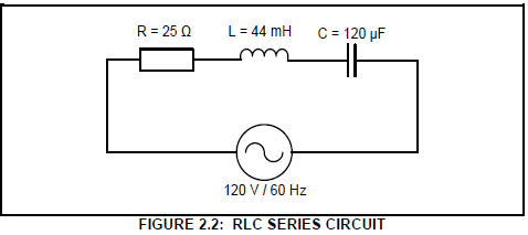
R = 25 Ω
L = 44 mH
C = 120 μF
VS = 120 V
f = 60 Hz
Calculate the:
2.2.1 Inductive reactance (3)
2.2.2 Capacitive reactance (3)
2.2.3 Impedance of the circuit (3)
2.3 FIGURE 2.3 below shows an RLC parallel circuit that consists of a 40 Ω resistor, an inductor with unknown inductance and a capacitor with a capacitive reactance of 60 Ω, all connected across a 220 V/60 Hz supply.
Answer the questions that follow.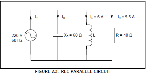
Given:
VS = 220 V L
F = 60 Hz
R = 40 Ω
XC = 60 Ω
IL = 6 A
IR = 5,5 A
2.3.1 Calculate the current through the capacitor. (3)
2.3.2 Calculate the reactive current. (3)
2.3.3 State, with a reason, whether the phase angle is leading or lagging. (2)
2.4 FIGURE 2.4 below shows an RLC series circuit that consists of a 12 Ω resistor, an inductor and a variable capacitor connected across a 120 V AC supply. The circuit resonates at 1 kHz. Answer the questions that follow.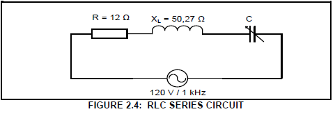
Given:
R = 12 Ω
XL = 50,27 Ω
VS = 120 V
fr = 1 kHz
2.4.1 State the value of the capacitive reactance at resonance. (1)
2.4.2 Calculate the value of the capacitor at resonance. (3)
2.4.3 Explain how the value of the current at resonance will be affected if the value of the resistance is doubled. (2)
2.5 A coil with a negligible resistance has an inductance of 80 mH and is connected in series with a 33 μF capacitor and a 30 Ω resistor. The circuit is then connected to a 120 V alternating supply with a variable frequency.
Given:
L = 80 mH
C = 33 μF
R = 30 Ω
VS = 120 V
Calculate the following:
2.5.1 Resonant frequency (3)
2.5.2 Current at resonance (3)
2.5.3 Voltage drop across the inductor at resonance if the inductive reactance is 49,24 Ω (3)
2.5.4 Explain why the voltage drop across the inductor at resonance is greater than the value of the supply voltage. (4)
[40]
QUESTION 3: SEMICONDUCTOR DEVICES (SPECIFIC)
3.1 Name TWO types of MOSFET. (2)
3.2 Refer to FIGURE 3.2 below that shows the output characteristic curve for both enhancement- and depletion-mode field-effect transistors. Answer the questions that follow.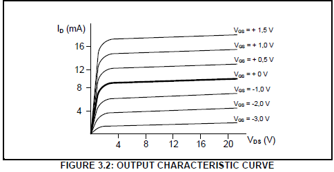
3.2.1 State the mode in which the MOSFET will operate for VGS > 0 V. (1)
3.2.2 Determine the drain-source current (IDS) in FIGURE 3.2 when the drain-source voltage (VDS) is 12 V and the gate-source voltage (VGS) is set to -2 V. (1)
3.2.3 Explain why the gate material represented by the output characteristic curve in FIGURE 3.2 above is a p-type material. (4)
3.3 Refer to FIGURE 3.3 below and answer the questions on the next page.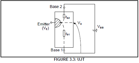
3.3.1 State the type of material used to produce the emitter substrate.(1)
3.3.2 State how the intrinsic standoff ratio is determined.(1)
3.3.3 Explain what happens when the voltage on the emitter terminal (VE) is increased above VX. (2)
3.4 FIGURE 3.4 below shows a Darlington pair transistor used as a switch.
Answer the questions that follow.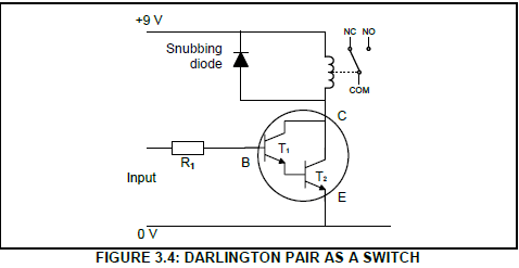
3.4.1 Write down the typical value of the base voltage needed across R1 to switch the Darlington pair ON. (1)
3.4.2 Calculate the voltage across the coil of the relay when the Darlington pair is switched ON. (3)
3.5 FIGURE 3.5 below shows two signals with the same frequency and amplitude that are applied onto the inputs of a 741 op amp. Answer the questions that follow.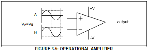
3.5.1 Write down the typical operating (supply) voltages of an op amp. (1)
3.5.2 Determine the value of the output voltage. (1)
3.5.3 Describe what will happen to the output signal if the amplitude of the signal on the non-inverting input is increased. (3)
3.6 Refer to FIGURE 3.6 below and answer the questions that follow.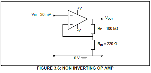
3.6.1 Identify the type of feedback in the circuit. (1)
3.6.2 Calculate the output voltage of the amplifier. (3)
3.7 FIGURE 3.7 below shows the internal block diagram of the 555 IC. Answer the questions that follow.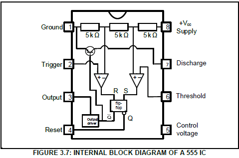
3.7.1 Name the THREE primary building blocks of the 555 IC. (3)
3.7.2 Explain the function of the three 5 kΩ resistors. (2)
[30]
QUESTION 4: SWITCHING CIRCUITS (GENERIC)
4.1 Explain the term bistable with reference to multivibrators. (1)
4.2 Refer to FIGURE 4.2 below and answer the questions that follow.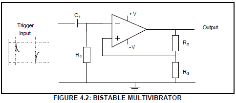
4.2.1 Draw the output signal with reference to the trigger input on ANSWER SHEET 4.2.1. (2)
4.2.2 Explain what happens in the circuit at switch-on until a trigger pulse is received. (3)
4.3 FIGURE 4.3 below shows the typical operating waveforms of a 741 op amp connected as a monostable multivibrator. Answer the questions that follow.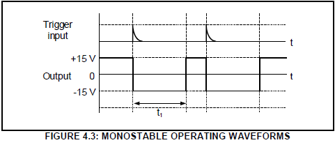
4.3.1 Explain what happens to the output with reference to t1 when a trigger input is received. (3)
4.3.2 State how the time period t1 can be varied. (2)
4.3.3 Explain the extent of the voltage swing at the output when a trigger pulse is received. (3)
4.4 Refer to FIGURE 4.4 below and answer the questions that follow.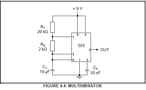
4.4.1 Identify the multivibrator in FIGURE 4.4 above. (1)
4.4.2 Draw the charging and discharging waveform of capacitor C1 on ANSWER SHEET 4.4.2. (3)
4.4.3 Explain why there is a difference in the charging and discharging times of the capacitor. (2)
4.4.4 Draw the output signal at pin 3 on ANSWER SHEET 4.4.4. (2)
4.5 Refer to FIGURE 4.5 below and answer the questions that follow.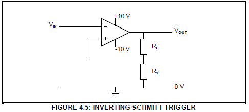
4.5.1 Explain the function of resistors RF and R1. (3)
4.5.2 Draw the output signal on ANSWER SHEET 4.5.2 if the signal in FIGURE 4.5.2 below is applied to the input of the Schmitt trigger.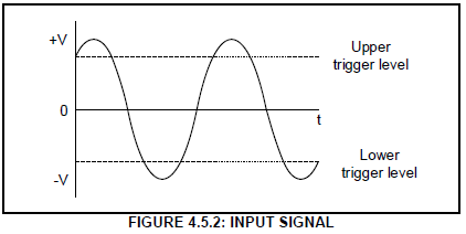
4.5.3 Describe how an increase in the value of RF will affect the trigger voltage. (3)
4.6 Refer to FIGURE 4.6 below and answer the questions that follow.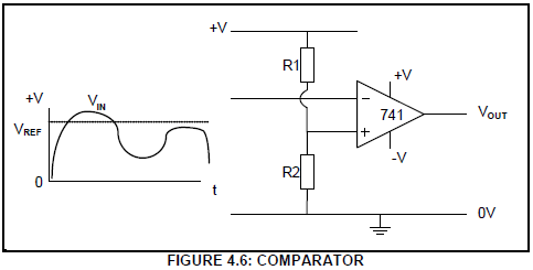
4.6.1 Explain what is meant by open loop with reference to FIGURE 4.6. (2)
4.6.2 Describe the principle of operation of a comparator. (6)
4.6.3 Draw the output signal on ANSWER SHEET 4.6.3. (2)
4.7 Refer to FIGURE 4.7 below and answer the questions that follow.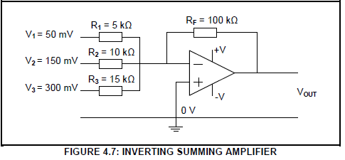
4.7.1 State how an additional input signal can be added to the summing amplifier. (1)
4.7.2 Calculate the output voltage for the inverting summing amplifier above. (3)
4.7.3 State why the answer to QUESTION 4.7.2 is negative. (1)
4.8 Refer to FIGURE 4.8 below and answer the questions that follow.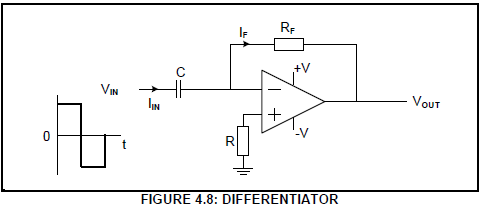
4.8.1 Give THREE reasons why it is advisable to connect an op amp to a passive RC differentiator. (3)
4.8.2 Draw the output signal on ANSWER SHEET 4.8.2. (2)
4.9 Give ONE reason for using a passive RC integrator circuit. (1)
4.10 FIGURE 4.10 below shows the output waveform of a passive RC-integrator displayed on the screen of an oscilloscope. Refer to the figure below and answer the questions that follow.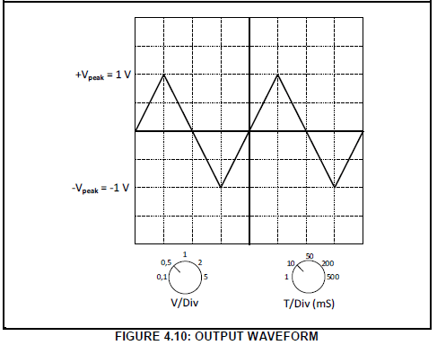
4.10.1 Identify the voltage per division setting. (1)
4.10.2 Determine the peak-to-peak voltage (3)
4.10.3 Determine how many complete cycles are displayed. (1)
4.10.4 Explain how a short RC time constant will affect the output of a passive RC integrator. (3)
[60]
QUESTION 5: AMPLIFIERS (SPECIFIC)
5.1 Explain why transistor amplifiers use a small signal stage at the input. (2)
5.2 Refer to FIGURE 5.2 below and answer the questions that follow.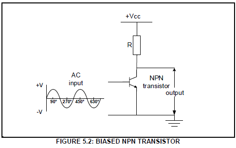
Draw the output waveform on ANSWER SHEETS 5.2.1 and 5.2.2 when the transistor is operating as a:
5.2.1 Class B amplifier(2)
5.2.2 Class AB amplifier(2)
5.3 State ONE advantage of negative feedback. (1)
5.4 Refer to FIGURE 5.4 below and answer the questions that follow.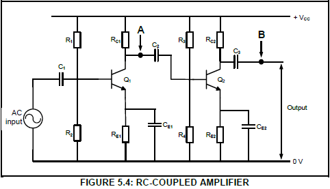
5.4.1 Identify the biasing method used in the amplifier above.(1)
5.4.2 State TWO functions of the biasing method in QUESTION 5.4.1. (2)
5.4.3 State the purpose of C1 and C2. (2)
5.4.4 Explain how C1, C2, and C3 will influence the voltage gain of an amplifier at lower frequencies.(2)
5.4.5 State THREE conditions that would cause distortion at the output. (3)
5.4.6 Draw the output signal at point A on ANSWER SHEET 5.4.6.(2)
5.4.7 State the phase relationship between the waveforms at point A and point B.(1)
5.5 Refer to FIGURE 5.5 below and answer the questions that follow.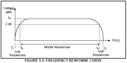
5.5.1 Define the term bandwidth of an amplifier.(2)
5.5.2 Identify the bandwidth.(1)
5.5.3 Explain what is meant by roll-off with reference to the frequency response of an amplifier. (2)
5.6 Refer to FIGURE 5.6 below and answer the questions that follow.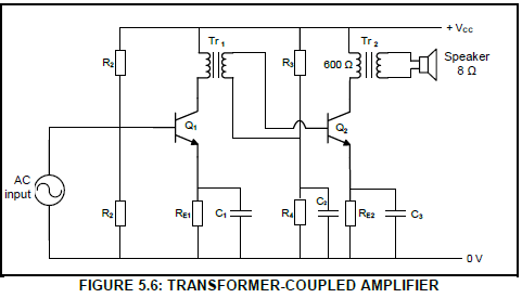
5.6.1 Explain why a transformer-coupled amplifier has less DC power loss at the collector when compared to a RC-coupled amplifier. (2)
5.6.2 Describe how impedance matching at output Tr2 is achieved. (2)
5.7 FIGURE 5.7 below shows an amplifier circuit. Answer the questions that follow.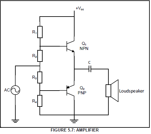
5.7.1 Identify the circuit.(2)
5.7.2 Explain how cross-over distortion can be eliminated in the circuit.(2)
5.7.3 Draw the output waveform on ANSWER SHEET 5.7.3.(2)
5.7.4 Explain the function of R1 and R2. (2)
5.8 The output power from an amplifier is 30 mW when the signal frequency is 2,5 kHz. When the frequency is increased to 7,5 kHz, the output power falls to 15 mW. Calculate the power gain in decibels after the frequency is increased.
Given:
POUT1 = 30 mW
POUT2 = 15 mW
f1 = 2,5 kHz
f2 = 7,5 kHz
5.9 FIGURE 5.9 below represents a radio-frequency amplifier. Answer the questions that follow.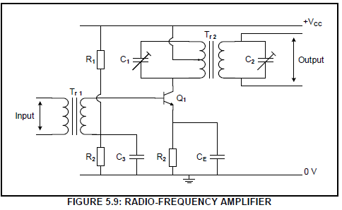
5.9.1 Explain the operation of the two LC circuits in the radio-frequency amplifier output stage.(5)
5.9.2 Draw a fully labelled frequency response curve of the RF-coupled amplifier on ANSWER SHEET 5.9.2.(4)
5.10 FIGURE 5.10 below shows a FET LC oscillator. Answer the questions that follow.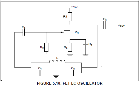
5.10.1 Define the term oscillator. (2)
5.10.2 Differentiate between the voltages that would develop across C1 and C2. (2)
5.10.3 State the function of the following components in FIGURE 5.10:
- R2 (1)
- C4 (1)
5.11 Refer to FIGURE 5.11 below, which shows an RC-phase shift oscillator using FET. Answer the questions that follow.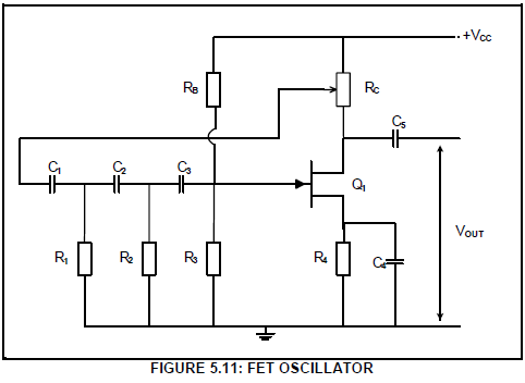
5.11.1 State TWO functions of the RC network. (2)
5.11.2 Describe how the frequency of the phase-shift oscillator can be adjusted. (3)
[60]
TOTAL: 200
FORMULA SHEET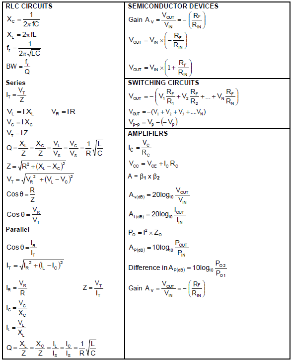
ANSWER SHEET 4.2.1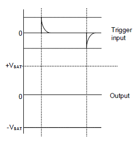
ANSWER SHEET 4.4.2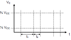
ANSWER SHEET 4.4.4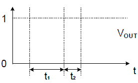
ANSWER SHEET 4.5.2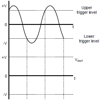
ANSWER SHEET 4.6.3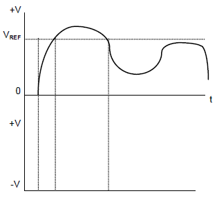
ANSWER SHEET 4.8.2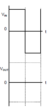
ANSWER SHEET 5.2.1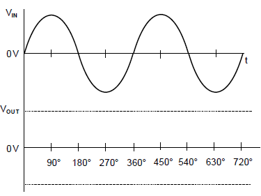
ANSWER SHEET 5.2.2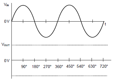
ANSWER SHEET 5.4.6
ANSWER SHEET 5.7.3
ANSWER SHEET 5.9.2