ELECTRICAL TECHNOLOGY:ELECTRONICS GRADE 12 MEMORANDUM - NSC PAST PAPERS AND MEMOS MAY/JUNE 2019
Share via Whatsapp Join our WhatsApp Group Join our Telegram GroupELECTRICAL TECHNOLOGY: ELECTRONICS
GRADE 12
NATIONAL SENIOR CERTIFICATE EXAMINATIONS
MEMORANDUM
MAY/JUNE 2019
INSTRUCTIONS TO THE MARKERS
- All questions with multiple answers imply that any relevant, acceptable answer should be considered.
- Calculations:
2.1 All calculations must show the formulae.
2.2 Substitution of values must be done correctly.
2.3 All answers MUST contain the correct unit to be considered.
2.4 Alternative methods must be considered, provided that the correct answer is obtained.
2.5 Where an incorrect answer could be carried over to the next step, the first answer will be deemed incorrect. However, should the incorrect answer be carried over correctly, the marker has to re-calculate the values, using the incorrect answer from the first calculation. If correctly used, the candidate should receive the full marks for subsequent calculations.
2.6 Markers should consider that learner answers may deviate slightly from the guideline, depending on how and where in the calculation rounding off was used. - This marking guideline is only a guide with model answers. Alternative interpretations must be considered and marked on merit. However, this principle should be applied consistently throughout the marking session at ALL marking centres.
QUESTION 1: OCCUPATIONAL HEALTH AND SAFETY (GENERIC)
1.1 An accident is an unplanned, uncontrolled event ✓ caused by unsafe acts and or unsafe conditions ✓ resulting in a personal injury, illness or the death of an employee. ✓
An accident means an accident arising out of and in the course of an employee’s employment and resulting in personal injury, illness or the death of the employee.
Note: The definition in the textbook is flawed but will be accepted. (3)
1.2 Move in an orderly manner. ✓
Follow the evacuation route as displayed in your workshop. ✓
Move to the designated assembly point in a calm and orderly manner. (2)
1.3 To prevent oneself form being shocked, ✓ therefore precautions must be taken to isolate oneself when rendering assistance.
To prevent injury. (1)
1.4 A third degree burn occurs when all layers of skin have been burnt, ✓ causing permanent skin damage affecting fat, muscle and even bone. ✓
A serious burn deserves 1 mark (2)
1.5 A person who intentionally and recklessly interferes with equipment will cause damages ✓ and this will render equipment unsafe and compromise the safety of the user. ✓ (2)
[10]
QUESTION 2: RLC CIRCUITS (GENERIC)
2.1
2.1.1 Capacitive reactance is the opposition ✓ to an alternating current by the reactive component of a capacitor ✓ in an ac circuit. (2)
2.1.2 Inductive reactance is the opposition ✓ to an alternating current by the reactive component of an inductor ✓ in an ac circuit.
If only the formula is given by the learner = 1 mark
If the formula is accompanied by the correct explanation = 2 marks. (2)
2.2
2.2.1 XL x 2 x π x f x L
= 2 x π x 60 x 44 x10-3
= 16,59 Ω ✓ (3)
2.2.2 XC = 1
2 x π x f x C
= 1 ✓
2 x π x 60 x120 x10-6
= 22,1 Ω (3)
2.2.3 Z √R2 + (XC - XL)2
= √252 + (22.11- 16.59)2
= 25,6 Ω ✓ (3)
2.3
2.3.1 IC = VS
VC
= 220
60
= 3,67 A ✓ (3)
2.3.2 IX = IL - IC
= 6 - 3,67
= 2,33 A ✓ (3)
2.3.3 The phase angle is lagging ✓ because IL is greater than IC.✓ (2)
2.4 2.4.1 At resonance frequency XL = XC
XC = 50,27 Ω (1)
2.4.2 C = 1
XC x 2π x f
= 1
50,27 x 2π x1000
= 3,17 x 10-6
= 3,17 μF (3) ✓
2.4.3 The value of the current will be halved as the circuit resistance is inversely proportional to the applied voltage. ✓
The value of the current will be halved if the resistance is doubled = 1 mark (2)
2.5
2.5.1 fr = 1
2π √L x C
= 1
2π √80 x 10-3 x 33 x 10-6
= 97,95 Hz (3)
2.5.2 I = VS (Z = R at resonance)
Z
= 120
30
= 4 A (3) ✓
2.5.3 VL = I x XL
= 4 x 49,24
= 196,94 V (3)
2.5.4 The voltage across XL is VL = IXL=. ✓
During resonance current is at a maximum. ✓
As a result VL would be higher due to the current being at a maximum. ✓ However because VL = VC the reactive voltage is zero ✓and effectively this voltage increase does not affect the supply voltage.
XL is greater than R, therefore VL will be greater than VR during resonance because the current in a series circuit is common through all components leading to the voltage across the inductor being greater than the supply voltage. (4)
[40]
QUESTION 3: SEMICONDUCTOR DEVICES (SPECIFIC)
3.1 N-channel depletion mode MOSFET
P-channel depletion mode MOSFET
N-channel enhancement mode MOSFET
P-channel enhancement mode MOSFET (2)
3.2
3.2.1 Enhancement mode(1)
3.2.2 +/- 4 mA (1)
3.2.3
- When a rising negative voltage (-VGS) is applied to the gate, the drain-source current (IDS) decrease.
- When a rising positive voltage (+VGS) is applied to the gate the drain-source current (IDS) increase.
This confirms that the gate material is p-type which is forward biased by a positive voltage and reverse biased by a negative voltage. (4)
3.3
3.3.1 The emitter is a heavily doped p-type semi-conductor. (1)
3.3.2 The intrinsic standoff ratio is determined by the ratio of the internal resistances (rb1 to rb1 + rb2)
The formula will be accepted as correct. (1)
3.3.3 The moment the emitter voltage (VE) is increased to above VX the UJT is said to 'fire' and goes into its 'trigger' state. (2)
3.4
3.4.1 1,4 V (1)
3.4.2 Normally VCE = 0,9 V when switched ON. therefore, VLOAD = VSUPPLY - VCE
= 9 - 0,9
= 8,1 V
Any VCE voltage from 0,3 to 2 V will be accepted as correct. (3)
3.5
3.5.1 +5 V/-5 V to +15 V/-15 V (1)
3.5.2 0 V (common mode rejection) (1)
3.5.3
- If the amplitude of the signal on the non-inverting input is increased, the Op-amp will amplify the difference between the two inputs.
- Because the non-inverting input is bigger than the inverting input,
- The output signal will now be in phase with the non-inverting input (3)
3.6
3.6.1 Negative feedback (1)
3.6.2  (3)
(3)
3.7
3.7.1 Two comparators/amplifiers
One R/S flip-flop
Three 5 kΩ resistors
Transistor (3)
3.7.2 The three 5 kΩ resistors divides the supply voltage into two stepped down voltages of 1/3 and 2/3 of the supply voltage (2)
[30]
QUESTION 4: SWITCHING CIRCUITS (GENERIC)
4.1 Bistable refers to two stable states, either high or low in multivibrators. (1)
4.2
4.2.1 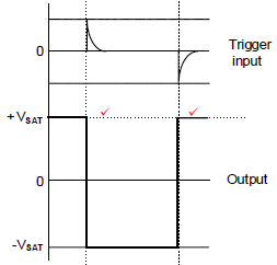
NOTE R1 acts as a pull down resistor ensuring that during switch on, the output will start at +VSAT
If the output is drawn inverted, 1 mark will be awarded for identifying both correct trigger points. (2)
4.2.2
- At switch-on, the voltage on the inverting input is zero ü while a small voltage from the voltage divider appears at the non-inverting terminal.
- This immediately drives the Op-amp into a state of positive saturation
- Where it will remain until a trigger pulse is received.
R1 acts as a pull down resistor ensuring that during switch on, the output will start at +VSAT (3)
4.3
4.3.1
- When a trigger input is received the output will change from positive saturation to negative saturation.
- It will remain in this state for a pre-determined time (t1).
- and then return back to its original state.
If the learner mentions a square wave, 1 mark is awarded (3)
4.3.2 The switched time can be varied by changing the value of either the resistor ü or capacitor ü in the charging RC-circuit. (2)
4.3.3
- In the resting condition the output is driven to positive saturation (+15 V).
- When a trigger pulse is received, the output of the switching current will switch to negative saturation (-15 V).
- Therefore the change in voltage from positive saturation to negative saturation adds up to a total change of 30 V. (3)
4.4
4.4.1 Astable multivibrator (1)
4.4.2
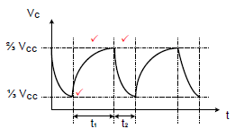 (3)
(3)
4.4.3 The capacitor charges through (R1+R2), causing a long RC time constant, but discharges through only R2 causing a short time constant. (2)
4.4.4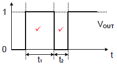
NOTE: If the output is inverted, 1 mark will be awarded for identifying both trigger points correctly. (2)
4.5
4.5.1
- RF and R1 create a voltage divider.
- They divide the output voltage to produce a small fraction of the output voltage across R1.
- This small fraction is fed to the Op-amp's non-inverting input. (3)
4.5.2 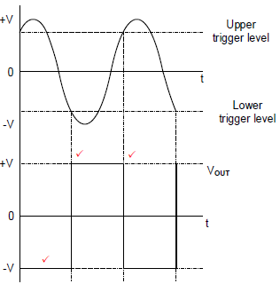
NOTE:
1 mark = correct orientation
2 marks = 1 mark for each correctly identified trigger point. (3)
4.5.3
- If the value of RF increases, the voltage across R1 will decrease according to Kirchhoff's voltage law.
- Therefore, the voltage fed back to the non-inverting input will decrease.
- This will lead to a decrease in trigger voltage. (3)
4.6
4.6.1 Open loop is when there is no feedback ü link between the output and input of the circuit. (2)
4.6.2
- Voltage divider resistors R1 and R2 set up the reference voltage VREF.
- The reference voltage is fed back to the non-inverting input of the Op-amp.
- The comparator compares the input voltage VIN to the reference voltage VREF.
- The gain of the Op-amp is ±100 000 because of the open loop connection.
- Whenever there is a fraction of a millivolt difference between VIN and VREF.
- The Op-amp will be driven into either one of the saturation states. (6)
4.6.3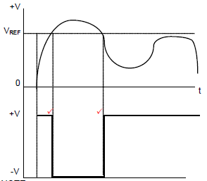
NOTE:
1 mark = correct orientation
1 mark = identifying both trigger points. (2)
4.7
4.7.1 By adding another input resistor to the summing amplifier input. (1)
4.7.2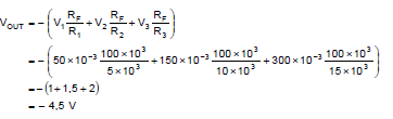 (3)
(3)
4.7.3 The answer in 4.7.2 is negative because the inputs are fed into the inverting input ü which will cause the output to be 180° out of phase. (1)
4.8
4.8.1 It improves input and output impedances.
It improves output gain.
It improves the stability of the circuit. (3)
4.8.2
This waveform is incorrectly given in the textbook, but must be accepted.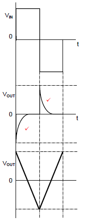
This is the correct output waveform of the Op-amp differentiator. (2)
4.9 A passive RC integrator is widely used in electronics to convert square waves into triangular waves. (1)
4.10
4.10.1 0,5 V per division.(1)
4.10.2 Vp-p = Vp -(-Vp) Vp-p= No.div x V per div
=1-(1) = 4 x 0.5V
=2 V = 2 V (3)
4.10.3
Two complete cycles (1)
4.10.4
- A short RC time constant will cause the capacitor to charge and discharge completely.
- This will resemble a square wave output signal with rounded leading and trailing edges. (3)
[60]
QUESTION 5: AMPLIFIERS (SPECIFIC)
5.1 Transistor amplifiers make use of a small signal stage at its input to enlarge a very low level signal üof voltage or current to a more manageable size, this reduces distortion ü into the output stage.
A small signal stage is used to amplify an input signal to drive the next stage of amplification.
To amplify the signal deserves only 1 mark (2)
5.2
5.2.1 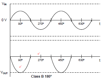 (2)
(2)
5.2.2 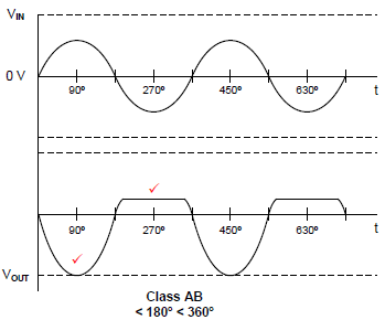 (2)
(2)
NOTE: If cross-over distortion is shown, the answer is correct.
5.3 Improved stability
More reliable and constant voltage gain
Can increase or decrease input and out impedances
Decrease distortion of the signal
Increased bandwidth (1)
5.4
5.4.1 Voltage divider base biasing. (1)
5.4.2 It sets up the operating conditions of the transistor.
It stabilises the transistor's operating point. (2)
5.4.3 C1 allows ac signals to pass in the input but stops any DC signals that might upset the bias arrangement.
C2 allows the AC in the output to pass to the next stage but blocks the DC signals.
Alternative for C2 Used as coupling between the two stages. (2)
5.4.4 The coupling capacitors cause the voltage gain to reduce due to an increase in reactance ü at lower frequencies. (2)
5.4.5 Distortion occurs if the steady bias voltage and current are too low (cut off) or too high (saturation) ü or the AC input is too large (3)
5.4.6 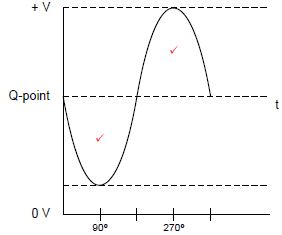 (2)
(2)
5.4.7 The waveform at point B will be 180° out of phase with the waveform at point A. (1)
5.5
5.5.1 The bandwidth of an amplifier is the range of frequencies within which the gain (A) does not fall below 0,7 of its maximum value (Amax)
Alternatively – The bandwidth of an amplifier is the range of frequencies at the -3 dB points.
NOTE if a learner only states middle frequencies it warrants 1 mark. (2)
5.5.2 The bandwidth will be determined between F2 and F3 (middle frequencies) (1)
5.5.3 The rate of decrease in the gain ü of an amplifier above or below the bandwidth ü of the amplifier. (2)
5.6
5.6.1 The resistance of the transformer's primary winding is lower ü than the collector resistance of the RC coupled amplifier, therefore it causes less DC power loss in that stage. (2)
5.6.2 Impedance matching is done by matching the impedance of the primary windings in Tr2 with the impedance of the loudspeaker at 8 Ω. (2)
5.7
5.7.1 Complimentary push-pull pair ü class AB amplifier. (2)
5.7.2 Cross-over distortion can be eliminated by biasing the two transistors Q1 and Q2 into class AB mode.
Adding a decoupling capacitor on the input will prevent the negative cycle on the input from draining the biasing to earth thus causing distortion.
By adding two diodes in the place of R2 and R3. (2)
5.7.3 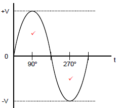 (2)
(2)
5.7.4 R1 and R2 forms a voltage divider circuit used to forward bias transistor Q1 (2)
5.8 AP = 10log10 (POUT2)
POUT 1
= 10log10 ( 15 x 10-3)
30 x 10-3
= 10log10 (0.5)
= -3.01dB (3)
5.9
5.9.1
- The first LC circuit (variable capacitor C1 and primary winding of Tr2) will resonate at the required frequency which is passed to the second stage and suppress other frequencies.
- The second LC circuit (variable capacitor C2 and the secondary winding of Tr2) makes the circuit more frequency selective
- This enables the circuit to be tuned to a variety of frequencies. (5)
5.9.2 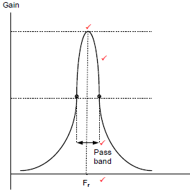 (4)
(4)
5.10
5.10.1 An oscillator is a device which generates an AC output signal without any externally applied input signal (2)
5.10.2 The voltage developed across C2 is the feedback voltage and the voltage developed across C1 is the oscillator's output voltage fed into the gate of the FET.(2)
5.10.3
- Resistor R2 is used for biasing the transistor when the circuit is switched ON. (1)
- C4 is used for stabilising the emitter voltage during the switching on of the transistor. (1)
5.11
5.11.1 The RC network provides a 180° phase shift.
It also determines the oscillation frequency of the circuit (2)
5.11.2 To adjust the frequency of the phase-shift oscillator it will be necessary to operate the three feedback capacitors as a single ganged component so that all the three capacitor values are adjusted to the same value. (3)
[60]
TOTAL: 200