ELECTRICAL TECHNOLOGY: ELECTRONICS GRADE 12 MEMORANDUM - NSC EXAMS PAST PAPERS AND MEMOS NOVEMBER 2018
Share via Whatsapp Join our WhatsApp Group Join our Telegram GroupELECTRICAL TECHNOLOGY: ELECTRONICS
GRADE 12
NSC EXAMS
PAST PAPERS AND MEMOS NOVEMBER 2018
MEMORANDUM
QUESTION 1: OCCUPATIONAL HEALTH AND SAFETY
1.1
- 'Major incident 'is an occurrence of catastrophic proportion✔ resulting from the use of plant and machinery from activities in the workplace. ✔
- Severe or serious injury or great damage to machinery and persons resulting from the use of plant or machinery in a workplace. (2)
1.2
- Manufacturers must ensure that products are safe ✔
- Not permitting any employee to do any work or to produce any artefact unless precautionary measures are in place. ✔
- Safe to use / without risk to health
- Safety feature
- Instructional manual
- Good state or design without a fault. (2)
1.3
- 'Horseplay' is an unsafe act because it is an inappropriate behaviour by learners ✔ in the workshop that would compromise the safety ✔ of themselves and others.
- It distracts others that could lead to accidents or incidents. (2)
1.4
- Do not touch the person. ✔
- Switch off the supply. ✔
- Help the person by removing him/her with a type of insulation material. (2)
1.5 Qualitative risk analysis defines the levels of threat ✔ and devises counter measures ✔ to eliminate possible risk. (2) [10]
QUESTION 2: RLC CIRCUITS
2.1 The total opposition to the flow of alternating current ✔ in a circuit comprising of resistance and reactance. ✔ (2)
2.2
2.2.1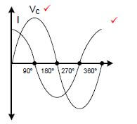 (2)
(2)
If the learner drew only one signal, it doesn’t show relation. (no marks)
2.2.2 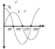 (2)
(2)
NOTE. If the learner drew only one signal, it doesn’t show relation. (no marks)
2.3
2.3.1
- C = 1
2 × π f × XC
= 1
2 × π × 60 × 36
= 73,68μF ✔ (3)
NOTE. Note if the formula is copied directly from the formula sheet a mark must be awarded, there after the substitution, manipulation and the answer must be correct to receive 3 marks.
2.3.2
- L = XL
2 × π × 60
= 22
2 × π × 60
= 58,35 mH ✔ ✔ (3)
NOTE. Note if the formula is copied directly from the formula sheet a mark must be awarded, there after the substitution, manipulation and the answer must be correct to receive 3 marks.
2.3.3 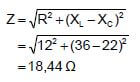 (3)
(3)
2.3.4
- 1 = VS
Z
= 60
18.44
= 3,25 A ✔ ✔ (3)
2.3.5
- Q = V × I × Sinθ
= 60 × 3,25 × Sin(50º) ✔
= 149,38 VA r ✔ (3)
2.4 The value of the inductive reactance will double/increase ✔ because the inductive reactance is directly proportional to the frequency ✔ of the supply voltage.
NOTE. If only the formula is given, no marks.
If the formula is given as a reason, 1 mark will be awarded for the formula. (2)
2.5. The resonant frequency is the frequency at which the inductive reactance ✔ is equal to the capacitive reactance. ✔
NOTE. All characteristics of resonance explained correctly will be accepted. (2)
2.6
- XL = VS
IL
=100
2
= 50 Ω (3) - XC = VS
IC
=100
6
= 16,67 Ω ✔ (3) - IX = IC + IL
= 6 - 2
= 4 A ✔ (3)
NOTE. If the learner stated either one or a difference in reactive currents is stated, the learner must be awarded 3 marks.  ✔ (3)
✔ (3)
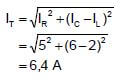 ✔ (3)
✔ (3) 2.6.2 Phase angle is leading. ✔ (1)
2.7 A low value of resistance produces a high Q-factor ✔ which results in a low bandwidth ✔ and high selectivity. (2) [40]
QUESTION 3: SEMICONDUCTOR DEVICES
3.1
- N-channel JFET or NFET ✔
- P-channel JFET or PFET ✔ (2)
3.2 To overcome leakage current between the gate terminal and Drain-Source channel, the gate terminal is electrically isolated from the channel ✔ by means of an extremely narrow layer of metal-oxide-silicon ✔ (MOS). (2)
3.3
3.3.1 Enhancement-mode ✔ N-channel ✔ MOSFET (2)
3.3.2 The lamp will switch ON as soon as the gate voltage VGS is raised ✔ to a sufficient level which will forward bias the internal channel of the MOSFET. ✔ (2)
3.3.3
- If RGS is short circuited, it will cause the internal conductive channel of the MOSFET to disperse, ✔ cutting the current flow ✔ and switching the lamp OFF. ✔ (3)
- If RGS is short circuited, the gate of the MOSFET will be tied directly to ground (0V potential), causing the internal channel to close and switch the lamp off.
3.4
3.4.1 Saturation region ✔ (1)
3.4.2
- At point C the UJT triggers ON. As the UJT is triggered, its internal resistance and voltage ✔ will decrease ✔ while current increases. ✔
- This is contrary to Ohm's law and is called negative resistance. (3)
3.5
3.5.1 Darlington pair ✔ (1)
3.5.2
- Very high current gain ✔
- Improved input impedance ✔
- When used in common collector pair it develops a very low output impedance (2)
3.6
3.6.1 Non-inverting input ✔ (1)
3.6.2
- Dual-in-line package outline (DIP) ✔
- Surface mount package (SMP) (1)
3.6.3  (2)
(2)
Note. If a square wave is drawn and it shows the correct inversion, 2 marks will be awarded.
3.7
- Open loop gain is the gain of an Op-Amp without any feedback ✔ from the output to the input.
- Closed loop gain is the gain of an Op-Amp with feedback ✔ from the output to the input. (2)
3.8  ✔ (3)
✔ (3)
3.9
- Trigger pin 2 is an active low trigger. ✔
- When the voltage on pin 2 is less than 1/3 of the supply voltage, the output goes high. ✔
- When the voltage is higher than 2/3 of the supply voltage, the output resets. ✔ (3) [30]
QUESTION 4: SWITCHING CIRCUITS
4.1
- An astable multivibrator generates a continuous train ✔ of (clock) pulses ✔ without the need of a trigger pulse.
- Continuously changes its state from high to low and back (2 marks)
- Continuously switches something on and off. (2 marks) (2)
4.2
4.2.1 Bistable multivibrator ✔ (1)
4.2.2 Positive feedback ✔ (1)
4.2.3 When a positive pulse (trigger pulse 1) is applied to the Trigger input, the output will change to a negative (-V) ✔ and remain there until a negative pulse (trigger pulse 2) is applied. ✔ When a negative pulse is applied to the trigger input, the output will change to positive. ✔ (3)
4.3
4.3.1
- Clock pulse generator ✔
- Morse code generators
- Timers
- Amateur radio equipment
- Systems that require square wave (1)
4.3.2  (2)
(2)
4.3.3
- If the value of R1 is increased, the RC time constant of the charging circuit (t1) increases, ✔ keeping the output of the 555 IC high for longer. ✔ This means that the positive output pulse (high) will be longer than the negative output pulse (low). ✔ (3)
- When the first trigger pulse is applied, Pin 7 of the 555 will be pulled (set) high to allow the capacitor to start charging. The charging period of the capacitor will only end once it has reached 2/3 Vcc, and any other further applied pulses during this period will be of no effect.
4.4
4.4.1  (4)
(4)
NOTE. Inverted polarity with correct intervals minus two marks
4.4.2 Trigger pulse B appears like a train of 'on' - 'off' pulses ✔ which is known as contact switch bounce. ✔ Switch bounce (2 marks) (2)
4.4.3
- The application of additional short pulses, ✔ after the initial set pulse will not affect the mono-stable multivibrator✔ that is already in the set state✔ and hence will not affect the charging of the capacitor (3)
- When the first trigger pulse is applied, Pin 7 of the 555 will be pulled (set) high to allow the capacitor to start charging. The charging period of the capacitor will only end once it has reached 2/3 Vcc, and any other further applied pulses during this period will be of no effect.
4.5
4.5.1
- Thermo-couple ✔
- Piezzo sensor ✔
- Microphone (2)
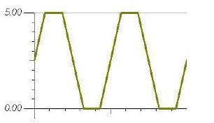
4.5.2 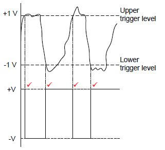 ✔ (4)
✔ (4)
4.5.3 When R1 is decreased the feedback voltage VR1 is decreased. ✔ As a result the positive feedback through R1 is decreased, ✔ lowering the trigger threshold voltage. ✔ (3)
4.6
4.6.1 The purpose of the comparator is to compare two input voltages. ✔ (1)
4.6.2
- A comparator compares the two voltages appearing at the two input terminals. ✔
- When one of its two input voltages is greater than the other, the output will go into one of the two saturation states. ✔
- When the inputs are reversed the output switches to the other saturation state. ✔ (3)
4.6.3 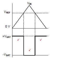 ✔ (3)
✔ (3)
4.7
4.7.1 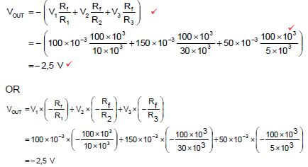 (3)
(3)
4.7.2 The voltage of each signal can be controlled independently by replacing each input resistor ✔ with a variable resistor ✔ (2)
4.7.3 DC blocking capacitors ✔ must be connected at the inputs ✔ to prevent dc current from being fed back to the input voltage sources. (2)
4.7.4 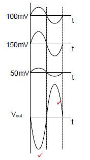
ONE mark for CORRECT POLARITY
ONE mark for AMPLIFICATION
If the wave form does not depict the wave size but there is reference to the correct value of the wave, a mark must be awarded (2)
4.8
4.8.1 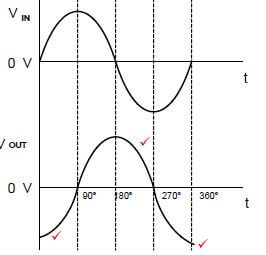
1 mark for 90° phase shift
Correct orientation of which will be:
- 1 mark for positive half
- 1 mark for negative half (3)
4.8.2 Triangular wave 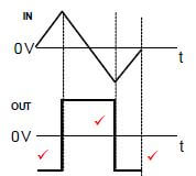
1 mark for phase shift ✔
2 marks for correct orientation (3)
4.9
4.9.1 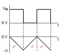 ✔ (3)
✔ (3)
4.9.2
- The textbook only mentioned the passive integrator of which the following will be accepted.
- If the RC time constant is short, the capacitor will charge rapidly ✔ reaching the maximum input voltage and remaining there ✔ until the input falls again. This results in the output having rounded leading and trailing edges ✔ with a flat top resembling a distorted square wave. ✔ (4)
- The following is the correct response for the Op-amp integrator.
- If the RC time constant is short, the output will rise in a linear manner until reaching the maximum output voltage and remaining there until the input falls again. This results in the output having straight sloping leading and trailing edges with flat tops and bottoms.
- It will resemble a triangular wave with its top and bottom peaks cut off. [60]

QUESTION 5: AMPLIFIERS
5.1 Class A - the transistor is biased with the Q-point on the midpoint ✔ of the load line, allowing for the full signal (360°) to be amplified. ✔ (2)
5.2
5.2.1
- To set the operating conditions (points) of the transistor. ✔
- To stabilise the operating point of the transistor. ✔ (2)
5.2.2 Q-point on the DC load line represents the voltages across the transistor ✔ and current through the transistor✔ when no input signal is applied. ✔ (3)
5.2.3 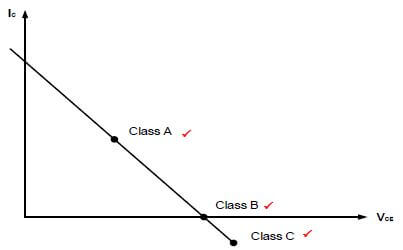 ✔ (3)
✔ (3)
Note. If the reference base biasing current is drawn and Q-point for class B is drawn slightly above line VCE, that mark will be awarded.
5.3 5.3.1 C2 serves as the AC coupling component between the two stages. ✔ C2 also blocks or decouples the DC component of the signal. ✔ (2)
5.3.2
- When an AC voltage is applied to the input of the first amplifier stage, ✔an alternating current will flow in the collector circuit of transistor (Q1). ✔
- An alternating voltage will develop across the collector resistor (RC1). ✔
- The developed alternating voltage across the RC1 will be transferred through capacitor C2 ✔ to the base of the transistor(Q2) in the amplifier 's second stage(stage 2). ✔
- The process will be repeated and the amplified output will measured between C3 and 0 V. ✔ (6)
5.3.3
- Impedance matching ✔
- Correct frequency response ✔
- DC isolation. (2)
5.4
5.4.1 Frequency response is the ability of the circuit ✔ to respond to a range of frequencies applied to the transistor. ✔ (2)
5.4.2 NOTE: The response given in the text book is wrong but marks will be awarded as such:
- Half-power points (-3dB) is the point when the output ✔ is at half the input power. ✔ (2)
- The correct response is as follows:
- The half-power point is the points at which the output power has dropped to half of its peak value; that is, at a level of -3 dB.
5.4.3
- At lower frequencies the reactances of the decoupling capacitors across the emitter resistors rises. ✔
- These reactances each combine with the resistance of their emitter resistors, causing the total impedance to rise ✔ limiting the stage gain. ✔ (3)
5.5
5.5.1 Impedance matching can be achieved by selecting a transformer ✔ with the required number of turns ✔ that will coincide with the impedances of the respective stages. (2)
5.5.2 The reason for using a transformer is that the relatively high output impedance of the second stage ✔ is connected to the relatively low impedance of the speaker ✔ thus matching the output impedance ✔ of the amplifier to the load. (3)
5.5.3 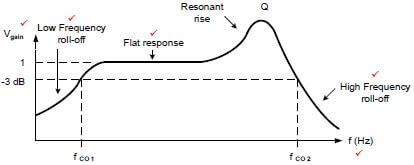 ✔ (6)
✔ (6)
5.6
5.6.1 An oscillator is a device which generates an AC output signal ✔ without any externally applied input signal. ✔ (2)
5.6.2 Sine wave ✔ (1)
5.6.3 Positive feedback ✔ (1)
5.6.4 The resistors R1 and R2 form a voltage divider ✔ to bias the base of the transistor. ✔ (2)
5.6.5
- The Colpitts oscillator uses TWO capacitors and an inductor in the tank circuit. ✔
- The Hartley oscillator uses TWO inductors and a capacitor in the tank circuit. ✔ (2)
5.7
5.7.1
- The transistor is used to amplify the damped oscillating signal ✔ ensuring a gain of 1 thus maintaining oscillation.
- Provide phase shift of 180°. ✔ (2)
5.7.2 The RC-network provides a phase shift of 180° ✔ and the amplifier circuit provides a phase shift of -180°. ✔ (2)
5.7.3 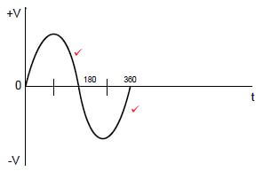 (2)
(2)
5.7.4
- No external input signal is applied to oscillators.✔
- The circuit is self-maintained.
- An input signal is required in the transistor amplifier.✔ (2)
5.8
- The RF-oscillator may be used in:
- Local oscillators ✔
- Radio circuits ✔
- Signal generator (2)
5.9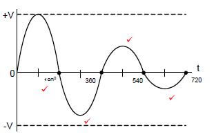
- 1 mark for constant frequency.
- 3 marks each half cycle with smaller amplitude. (4) [60]
TOTAL: 200