ELECTRICAL TECHNOLOGY: DIGITAL ELECTRONICS GRADE 12 QUESTIONS - 2018 SEPTEMBER PREPARATORY EXAM PAPERS AND MEMOS
Share via Whatsapp Join our WhatsApp Group Join our Telegram GroupELECTRICAL TECHNOLOGY: DIGITAL ELECTRONICS
GRADE 12
NATIONAL SENIOR CERTIFICATE
SEPTEMBER 2018
INSTRUCTIONS AND INFORMATION
- This question paper consists of FIVE questions.
- Sketches and diagrams must be large, neat and fully labelled.
- Show ALL calculations and round off answers correctly to TWO decimal places. Show the units for ALL answers of calculations.
- Number the answers correctly according to the numbering system used in this question paper.
- You may use a non-programmable calculator.
- A formula sheet is provided at the end of this question paper.
- Write neatly and legible.
QUESTION 1: OCCUPATIONAL HEALTH AND SAFETY
1.1 Summarise the purpose of the Occupational Health and Safety Act. (2)
1.2 Explain the ‘let-go’ current during an electrical shock.(2)
1.3 State ONE unsafe condition that must be avoided in a workshop. (1)
1.4 Give ONE unsafe act in a school workshop that can cause an accident. (1)
1.5 Describe TWO standard treatments for shock. (2)
[8]
QUESTION 2: SWITCHING AND CONTROL CIRCUITS
2.1 Refer to the figure below and answer the questions that follow.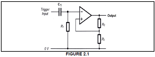
2.1.1 Identify the circuit diagram above. (1)
2.1.2 Describe the operation of the circuit above. (6)
2.1.3 Draw the input and output waveform diagrams of the circuit above. (4)
2.2 Draw a fully labelled circuit diagram of an op-amp mono-stable multivibrator. (4)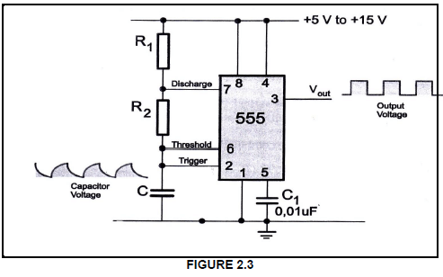
2.3.1 Identify the circuit diagram above. (1)
2.3.2 Explain briefly the operation of the circuit above. (4)
2.4 List FOUR applications of a Schmitt trigger. (4)
2.5
 (1)
(1)
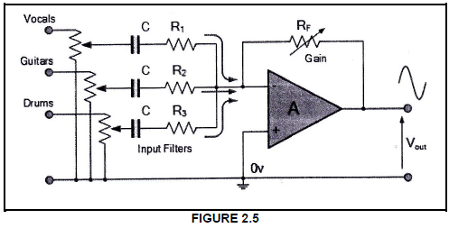
2.5.1 Identify the circuit in FIGURE 2.5.
2.5.2 If all four resistors in the circuit are set to exactly the same value of 10 kΩ and the three input voltages are: vocals = 200 mV, guitars = 250 mV and drums = 300 mV, calculate the final size of the output voltage. (3)
2.6 When an active Op Amp integrator has a very long time constant:
2.6.1 State what this means with regard to the components of the circuit. (1)
2.6.2 What shape of output wave form would be expected from this circuit if it was presented with a square wave? (1)
2.7 Draw a fully labelled circuit diagram of a 741 IC being used as a comparator in a light-sensing circuit. (6)
2.8 Draw both sinusoidal input and the waveform that would appear at the output of an active differentiator circuit when a sine wave is presented at its input. (4)
2.9 Discuss the main difference between a mono-stable multivibrator and a bi-stable multivibrator. (4)
2.10 Identify the TWO passive component circuits shown below.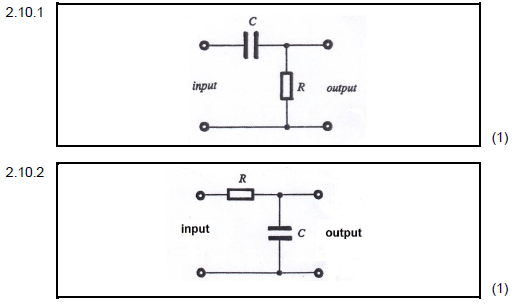
2.11 Critically analyse the operation of a passive RC differentiator. (6)
2.12 Explain how the resistor and capacitor affect the operation of a Passive RC integrator. (2)
2.13 Draw a circuit diagram of an active Op-Amp differentiator. (4)
[58]
QUESTION 3: SEMICONDUCTOR DEVICES
3.1 Explain why it is necessary for an Op-Amp to be supplied with both a positive and a negative power supply. (3)
3.2 Explain briefly how a 741 Op-Amp is constructed. (3)
3.3 Name TWO input terminals of an Op-Amp. (2)
3.4 Explain TWO advantages of using negative feedback with Op-Amp. (2)
3.5 Draw the circuit diagram showing two transistors coupled as a Darlington pair. (3)
3.6 A non-inverting Op-Amp circuit which has a 500 kΩ feedback resistor ?? and 10 kΩ resistor ??? coupled to 0V.
3.6.1 Calculate the voltage gain of the Op-Amp. (3)
3.6.2 State the effect of the input voltage to the output voltage. (1)
3.7 State ANY mode of operation of a 555 timer IC. (1)
[18]
QUESTION 4: DIGITAL AND SEQUENTIAL DEVICES
4.1 Give TWO types of seven segment display devices commonly available. (2)
4.2 Name the light altering principle that a liquid crystal display relies on. (1)
4.3 A combinational logic circuit combining an AND gate with an exclusive OR gate (XOR) creates the basic circuit for a computer’s binary single bit addition, the HALF ADDER circuit.
4.3.1 Design a half adder circuit using an AND-gate and an XOR-gate. (4)
4.3.2 Draw the circuit truth table for the above design. (4)
4.4 Give the difference between an encoder and a decoder. (2)
4.5 Briefly explain sequential logic circuit. (3)
4.6 Refer to figure 4.1.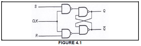
4.6.1 Identify the circuit diagram above. (1)
4.6.2 Draw the logic symbol for the circuit in FIGURE 4.1. (3)
4.6.3 Draw the truth table for a clocked circuit. (4)
4.7 Critically describe the difference between the asynchronous device and synchronous device. (5)
4.8 FIGURE 4.2 below represents a down counter.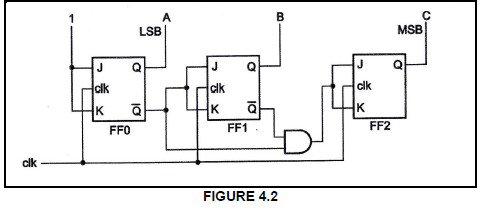
4.8.1 Explain the operation of a down counter. (3)
4.8.2 Draw the truth table for a three-bit synchronous down counter with the count starting at 1112 and decreasing on every successive clock pulse. (4)
4.9 What does the abbreviation BCD mean and how does it operate? (3)
4.10 Distinguish between full sequence counter and truncated counter. (2)
4.11 Draw the circuit block diagrams to describe how the following registers function:
4.11.1 Serial in: Parallel out (3)
4.11.2 Parallel in: Serial out (3)
4.12 Describe using diagrams, what is meant by a:
4.12.1 Sourcing output (2)
4.12.2 Sinking output (2)
4.13 Name THREE input combinations which can produce useful output states for Active Low Latch. (3)
4.14 Draw a three-stage asynchronous ripple counter’s timing diagram. (4)
[58]
QUESTION 5: MICROCONTROLLERS
5.1 Briefly explain a microcontroller. (3)
5.2 Sketch a fully labelled block diagram of a microcontroller. (4)
5.3 Give the correct name and a brief explanation of the functions of the following:
5.3.1 CPU (3)
5.3.2 RAM (3)
5.3.3 ROM (3)
5.4 Describe the main advantages of using a microcontroller. (3)
5.5 List the THREE types of busses in a processor. (3)
5.6 List TWO input sensors and TWO output transducers. (4)
5.7 Explain the difference between a microprocessor and a microcontroller. (2)
5.8 Describe a flowchart. (2)
5.9 Plan and draw a flowchart of steps to take to solder a component to a PCB. (5)
5.10 Using simple drawings, explain serial and parallel communications. (6)
5.11 Name THREE special purpose registers. (3)
5.12 Describe the term program when referring to computer programs. (2)
5.13 Explain what a register is with reference to a computer. (2)
5.14 Using drawings, explain each of the following types of communication:
5.14.1 Simplex (2)
5.14.2 Duplex (2)
5.14.3 Full-duplex (2)
5.15 Briefly explain the purpose of UART. (2)
5.16 Describe discreet logic (2)
[58]
TOTAL: 200
FORMULA SHEET
SWITCHING CIRCUITS
- Gain A?=???? =−(? ?) inverting operational amplifier
??? ??? - Gain A?=????=1+(? ?)non−inverting operational amplifier
??? ??? - ????=???×(−??) inverting amplifier
??? - ????=−(?1+?2+?3) summing up op-amp
- ??= 1
2?√?? - ?= 1
2?√6??