ELECTRICAL TECHNOLOGY: ELECTRONICS GRADE 12 QUESTIONS - NSC EXAMS PAST PAPERS AND MEMOS NOVEMBER 2018
Share via Whatsapp Join our WhatsApp Group Join our Telegram GroupELECTRICAL TECHNOLOGY: ELECTRONICS
GRADE 12
NSC EXAMS
PAST PAPERS AND MEMOS NOVEMBER 2018
INSTRUCTIONS AND INFORMATION
- This question paper consists of FIVE questions.
- Answer ALL the questions.
- Answer the following questions on the attached ANSWER SHEETS:
QUESTIONS 2.2.1 and 2.2.2
QUESTION 3.6.3
QUESTIONS 4.3.2, 4.4.1, 4.5.2, 4.6.3, 4.7.4, 4.8.1, 4.8.2 and 4.9.1 QUESTIONS 5.2.3, 5.5.3, 5.7.3 and 5.9 - Write your CENTRE NUMBER and EXAMINATION NUMBER on every ANSWER SHEET and hand them in with your ANSWER BOOK, whether you have used them or not.
- Sketches and diagrams must be large, neat and fully labelled.
- Show ALL calculations and round off answers correctly to TWO decimal places.
- Number the answers correctly according to the numbering system used in this question paper.
- You may use a non-programmable calculator.
- Show the units for ALL answers of calculations.
- A formula sheet is attached at the end of this question paper.
- Write neatly and legibly.
QUESTIONS
QUESTION 1: OCCUPATIONAL HEALTH AND SAFETY (GENERIC)
1.1 Define the term major incident with reference to the Occupational Health and Safety Act, 1993 (Act 85 of 1993). (2)
1.2 State TWO general duties of manufacturers with regard to a product that will be used at the workplace. (2)
1.3 Explain why horseplay is an unsafe act in the workshop. (2)
1.4 State TWO procedures that you have to follow to protect yourself when you help a person who is being shocked by electricity. (2)
1.5 Define the term qualitative risk analysis. (2) [10]
QUESTION 2: RLC CIRCUITS (GENERIC)
2.1 Define the term impedance with reference to RLC circuits. (2)
2.2 Illustrate the phase relationship between current and voltage by drawing the waveforms of the following circuits on ANSWER SHEET 2.2:
2.2.1 Pure capacitive circuit (2)
2.2.2 Pure inductive circuit (2)
2.3 FIGURE 2.3 below shows a RLC series circuit that consists of a 12 Ω resistor, an inductor with a reactance of 22 Ω and a capacitor with a reactance of 36 Ω, all connected across a 60 V/60 Hz supply. Answer the questions that follow. 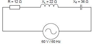
FIGURE 2.3: RLC SERIES CIRCUIT
Given:
- R = 12 Ω
XL = 22 Ω
XC = 36 Ω
VS = 60 V
f = 60 Hz
Calculate the:
2.3.1 Capacitance of the capacitor (3)
2.3.2 Inductance of the inductor (3)
2.3.3 Impedance of the circuit (3)
2.3.4 Total current through the circuit (3)
2.3.5 Reactive power at a phase angle of 50° (3)
2.4 Explain how the value of the inductive reactance will be affected if the supply frequency is doubled. (2)
2.5 Define the term resonant frequency. (2)
2.6 Refer to FIGURE 2.6 below and answer the questions that follow. 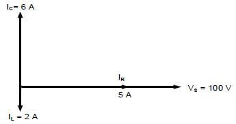
FIGURE 2.6: RLC PHASOR DIAGRAM
2.6.1 Calculate the following:
- Inductive reactance (3)
- Capacitive reactance (3)
- Reactive current (3)
- Total current (3)
2.6.2 State whether the phase angle is lagging or leading. (1)
2.7 Describe how a low resistance value affects the bandwidth of an LC tuned circuit. (2) [40]
QUESTION 3: SEMICONDUCTOR DEVICES (SPECIFIC)
3.1 Name TWO types of junction field effect transistors (JFETs). (2)
3.2 Explain how the construction of the JFET was modified to overcome the leakage current between the gate terminal and drain-source channel. (2)
3.3 Refer to FIGURE 3.3 below and answer the questions that follow. +VDD 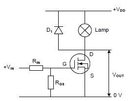
FIGURE 3.3: MOSFET AS A SWITCH
3.3.1 Identify the type of MOSFET used in this circuit. (2)
3.3.2 Explain when the lamp in this circuit will switch ON. (2)
3.3.3 Describe what will happen if RGS is short-circuited. (3)
3.4 FIGURE 3.4 below shows the characteristic curve of a UJT. Answer the questions that follow. 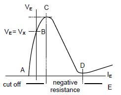
FIGURE 3.4: UJT CHARACTERISTIC CURVE
3.4.1 Identify region E. (1)
3.4.2 Explain what happens in the UJT between points C and D of the characteristic curve. (3)
3.5 Refer to FIGURE 3.5 below and answer the questions that follow. C 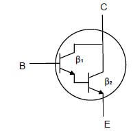
FIGURE 3.5: TRANSISTOR
3.5.1 Identify the configuration in which the transistors are connected. (1)
3.5.2 State TWO advantages of the transistor configuration in FIGURE 3.5. (2)
3.6 FIGURE 3.6 below shows the 741 op amp. Answer the questions that follow. 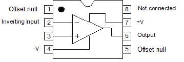
FIGURE 3.6: 741 OP AMP
3.6.1 Label pin 3. (1)
3.6.2 Name the type of package in which the integrated circuit (IC) above is constructed. (1)
3.6.3 Draw the output signal on ANSWER SHEET 3.6.3 if the signals in FIGURE 3.6.3 below are applied to the inputs of an op amp. 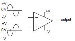
FIGURE 3.6.3: SIGNALS (2)
3.7 Explain the difference between open-loop gain and closed-loop gain with reference to op amps. (2)
3.8 Calculate the output voltage of the op amp in FIGURE 3.8 below. 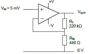
FIGURE 3.8: OP AMP
Given:
VIN = 5 mV
RIN = 440 Ω
RF = 220 kΩ (3)
3.9 Refer to FIGURE 3.9 below and explain the operation of the 555 timer when connected in monostable mode. 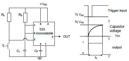
FIGURE 3.9: MONOSTABLE MULTIVIBRATOR (3) [30]
QUESTION 4: SWITCHING CIRCUITS (SPECIFIC)
4.1 Explain the purpose of an astable multivibrator. (2)
4.2 Refer to FIGURE 4.2 below and answer the questions that follow. 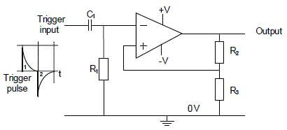
FIGURE 4.2: MULTIVIBRATOR
4.2.1 Identify the multivibrator in FIGURE 4.2. (1)
4.2.2 Name the type of feedback provided by R2. (1)
4.2.3 Describe the change in the output signal with reference to input trigger pulses 1 and 2. (3)
4.3 FIGURE 4.3 below shows the 555 IC astable multivibrator and the voltage graph of capacitor C1. Answer the questions that follow. 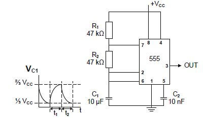
FIGURE 4.3: 555 IC ASTABLE MULTIVIBRATOR
4.3.1 Name ONE application of an astable multivibrator. (1)
4.3.2 Draw the output signal with reference to signal VC1 on ANSWER SHEET 4.3.2. (2)
4.3.3 Describe how an increase in the value of R1 will affect the output signal. (3)
4.4 FIGURE 4.4 below shows input trigger pulses A and B to a 555 monostable multivibrator. Answer the questions that follow. 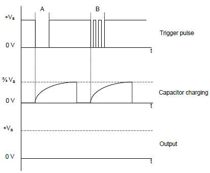
FIGURE 4.4: MONOSTABLE MULTIVIBRATOR TRIGGER PULSES
4.4.1 Draw the output signal on ANSWER SHEET 4.4.1. (4)
4.4.2 Describe the condition that occurred at trigger pulse B. (2)
4.4.3 Explain why the condition that occurs at trigger pulse B does NOT affect the capacitor charging. (3)
4.5 Refer to FIGURE 4.5 below and answer the questions that follow. 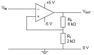
FIGURE 4.5: INVERTING SCHMITT TRIGGER
4.5.1 Name TWO transducers that can be used as input devices to the Schmitt trigger. (2)
4.5.2 Draw the output signal on ANSWER SHEET 4.5.2 if the input signal in FIGURE 4.5.2 below is applied to the circuit. 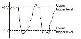
FIGURE 4.5.2: INPUT SIGNAL (4)
4.5.3 Describe how a decrease in the value of R1 will affect the trigger voltage level of the Schmitt trigger. (3)
4.6 FIGURE 4.6 shows the 741 op amp as a comparator. Answer the questions that follow. 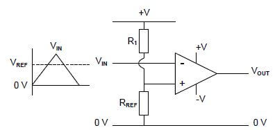
FIGURE 4.6: COMPARATOR
4.6.1 State the purpose of the comparator. (1)
4.6.2 Briefly explain how the comparator achieves its function. (3)
4.6.3 Draw the output signal on ANSWER SHEET 4.6.3, with reference to the input signal in FIGURE 4.6. (3)
4.7 Refer to FIGURE 4.7 below and answer the questions that follow. 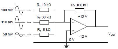
FIGURE 4.7: INVERTING SUMMING AMPLIFIER
4.7.1 Calculate the output voltage. (3)
4.7.2 Explain how this circuit can be modified to control the input voltage of each signal independently. (2)
4.7.3 Describe how this circuit can be modified to prevent DC from being fed back to the input voltage sources. (2)
4.7.4 Draw the output signal on ANSWER SHEET 4.7.4. (2)
4.8 FIGURE 4.8 below shows an op amp as a differentiator. Draw the output signals on ANSWER SHEET 4.8 when the signals, shown in QUESTIONS 4.8.1 and 4.8.2, are applied to the input of the circuit. 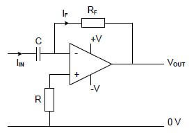
FIGURE 4.8: OP AMP AS DIFFERENTIATOR
4.8.1 Sine wave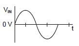 (3)
(3)
4.8.2 Triangular wave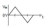 (3)
(3)
4.9 Refer to FIGURE 4.9 below and answer the questions that follow. 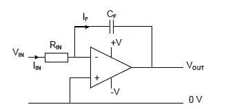
FIGURE 4.9: OP AMP AS INTEGRATOR
4.9.1 Draw the output signal on ANSWER SHEET 4.9.1, when the input signal in FIGURE 4.9.1 below is applied. 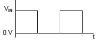
FIGURE 4.9.1: INPUT SIGNAL (3)
4.9.2 Describe what will happen to the output signal if the RC time constant is short. (4) [60]
QUESTION 5: AMPLIFIERS (SPECIFIC)
5.1 Describe class A amplification with reference to the biasing of a transistor. (2)
5.2 Refer to FIGURE 5.2 below and answer the questions that follow. 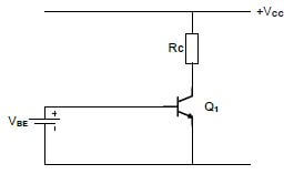
FIGURE 5.2: TRANSISTOR BIASING
5.2.1 Give TWO reasons for biasing a transistor. (2)
5.2.2 Explain the term Q-point on a DC load line. (3)
5.2.3 Indicate the Q-point of a class A, class B and class C amplifier on ANSWER SHEET 5.2.3. (3)
5.3 Refer to FIGURE 5.3 below and answer the questions that follow. 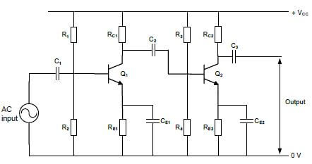
FIGURE 5.3: RC-COUPLED AMPLIFIER
5.3.1 State TWO functions of capacitor C2. (2)
5.3.2 Describe the operation of an RC-coupled amplifier. (6)
5.3.3 State TWO requirements of the coupling of amplifier stages. (2)
5.4 Analyse FIGURE 5.4 below and answer the questions that follow. 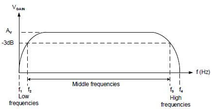
FIGURE 5.4: FREQUENCY RESPONSE OF RC-COUPLED AMPLIFIER
5.4.1 Define the term frequency response with reference to amplifiers. (2)
5.4.2 Explain the term half-power points with reference to a frequency response curve. (2)
5.4.3 Describe how the voltage gain of an RC-coupled amplifier is affected at low frequencies. (3)
5.5 Refer to FIGURE 5.5 below and answer the questions that follow. 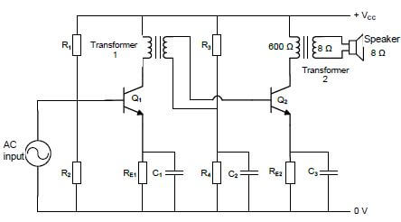
FIGURE 5.5: TRANSFORMER-COUPLED AMPLIFIER
5.5.1 Describe how proper impedance matching can be achieved between the transistor of the first stage and the transistor of the second stage. (2)
5.5.2 Explain why a transformer is used at the output of the amplifier. (3)
5.5.3 Draw the output frequency response curve of the amplifier circuit on ANSWER SHEET 5.5.3. (6)
5.6 Refer to FIGURE 5.6 below and answer the questions that follow. 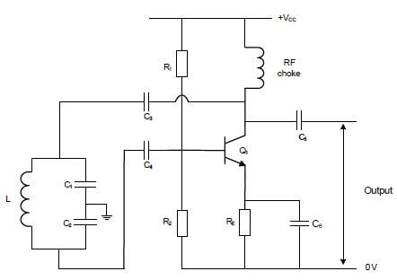
FIGURE 5.6: COLPITTS OSCILLATOR
5.6.1 Define the term oscillator. (2)
5.6.2 Name the type of waveform that is generated by an oscillator. (1)
5.6.3 Name the type of feedback used in FIGURE 5.6. (1)
5.6.4 State the purpose of resistors R1 and R2 in the circuit. (2)
5.6.5 Differentiate between the Hartley oscillator and the Colpitts oscillator with reference to the tank circuits. (2)
5.7 FIGURE 5.7 below shows an RC phase-shift oscillator circuit diagram. Answer the questions that follow. 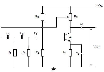
FIGURE 5.7: RC-PHASE-SHIFT OSCILLATOR
5.7.1 State TWO functions of the transistor in the circuit. (2)
5.7.2 Explain why the total phase shift of the oscillating circuit is zero. (2)
5.7.3 Draw the output waveform of the RC-oscillator on ANSWER SHEET 5.7.3. (2)
5.7.4 Differentiate between oscillator circuits and transistor amplifier circuits with reference to input signals. (2)
5.8 Give TWO examples of where an RF-oscillator can be used. (2)
5.9 Draw TWO cycles of damped oscillation on ANSWER SHEET 5.9. (4) [60]
TOTAL: 200
FORMULA SHEET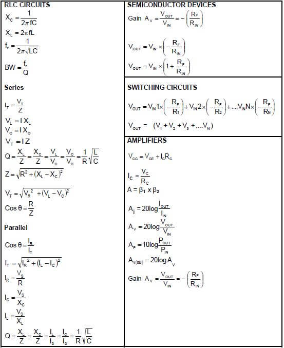
EXAMINATION NUMBER: |
CENTRE NUMBER: |
ANSWER SHEET 2.2 
FIGURE 2.2.1 (2)
FIGURE 2.2.2 (2)
EXAMINATION NUMBER: |
CENTRE NUMBER: |
ANSWER SHEET 3.6.3 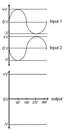
FIGURE 3.6.3 (2)
EXAMINATION NUMBER: |
CENTRE NUMBER: |
ANSWER SHEET 4.3.2 Input 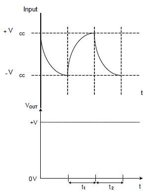
FIGURE 4.3.2 (2)
EXAMINATION NUMBER: |
CENTRE NUMBER: |
ANSWER SHEET 4.4.1 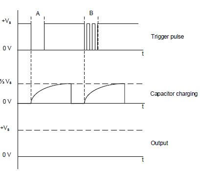
FIGURE 4.4.1 (4)
EXAMINATION NUMBER: |
CENTRE NUMBER: |
ANSWER SHEET 4.5.2 +1 V 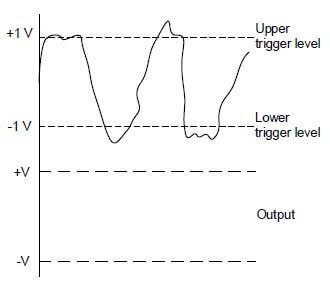
FIGURE 4.5.2 (3)
EXAMINATION NUMBER: |
CENTRE NUMBER: |
ANSWER SHEET 4.6.3 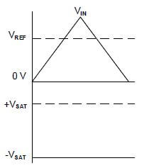
FIGURE 4.6.3 (3)
EXAMINATION NUMBER: |
CENTRE NUMBER: |
ANSWER SHEET 4.7.4 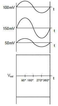
FIGURE 4.7.4 (2)
EXAMINATION NUMBER: |
CENTRE NUMBER: |
ANSWER SHEET 4.8 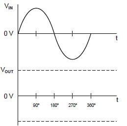
FIGURE 4.8.1 (3) 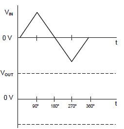
FIGURE 4.8.2 (3)
EXAMINATION NUMBER: |
CENTRE NUMBER: |
ANSWER SHEET 4.9.1 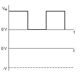
FIGURE 4.9.1 (3)
EXAMINATION NUMBER: |
CENTRE NUMBER: |
ANSWER SHEET 5.2.3 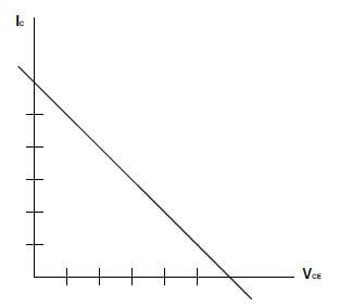
FIGURE 5.2.3 (3)
EXAMINATION NUMBER: |
CENTRE NUMBER: |
ANSWER SHEET 5.5.3 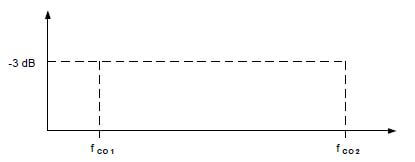
FIGURE 5.5.3 (6)
EXAMINATION NUMBER: |
CENTRE NUMBER: |
ANSWER SHEET 5.7.3 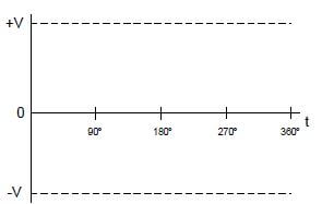
FIGURE 5.7.3 (2)
EXAMINATION NUMBER: |
CENTRE NUMBER: |
ANSWER SHEET 5.9 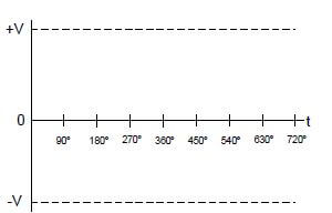
FIGURE 5.9 (4)